

StructSure™
Photoresists & Specialty Chemicals
Photoresists & Specialty Chemicals
Passivation
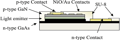
Part of the Applications Notes LinePassivation is the process of depositing a thin inert film onto the surface of a micro device in order to greatly improve its electrical characteristics. SU-8 passivation enhances device performance of small area diodes which are susceptible to surface area effects. Surface leakage currents due to abrupt termination of crystal structure, dangling bonds, inversion layer, and interfacial traps at the device/air interface can be overcome by using SU-8 passivation.
HgCdTe and newer type-II InAs/GaSb superlattice (T2SL) IR imagers benefit from SU-8 passivation. GaN Light Emitting Diodes (LEDs) performance is also greatly enhanced.
SU-8: Benefits/Attributes
- Easily integrates into fabrication process
- Improves device performance by reducing dark current density
- High aspect ratio imaging
- 0.5 to >200µm in a single coat
- Superb chemical and temperature resistance
- Optical transparency
- Hydrophobic surface after cross-linking
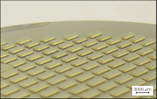
Passivation layer for diodes.
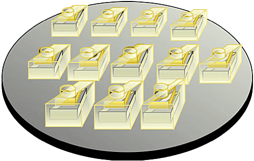
Encapsulation with imaged vias.
FEATURED APPLICATIONS