High‑temp sputtering for low‑loss optical films often deforms standard resists. A study shows a thermally robust LOR C + UniLOR® N bilayer system enabling reliable lift‑off during high‑temperature dielectric deposition.
Introduction
Modern optical and photonic devices increasingly rely on dense, low‑loss dielectric films, that can withstand high temperatures. While sputtering at elevated temperatures is ideal for achieving the right refractive index and stoichiometry, it introduces a major fabrication challenge: most photoresists cannot survive these extreme thermal and mechanical stresses, causing deformation, collapse, or failed lift‑off.
A recent study done in-house by Kayaku Advanced Materials in collaboration with Bühler Leybold Optics, using their HELIOS 800 sputter coater to deposit the metal oxides, demonstrates a solution: a thermally robust bi‑layer lift‑off resist system built with LOR C and UniLOR® N, engineered specifically for high temperature sputtering of dielectric optical films.
Why Lift-off Matters for Optical Filters
Patterning dielectric layers using lift‑off is becoming increasingly essential because:
- Many optical materials (SiO₂, TiO₂, Al₂O₃, Nb₂O₅, etc.) cannot be cleanly etched using plasma or wet processes.
- Optical coatings often involve <10 micron, multi‑layer stacks, which place high stress on resist structures.
- Sputtering at ≥180°C is required for optical grade, stoichiometrically stable films, but standard resists soften, flow, and degrade.
Conventional positive- and negative-tone photoresists simply aren’t built to withstand these conditions.
The Bi-Layer Solution: LOR C + UniLOR® N
The engineering teams designed a bi‑layer lift‑off stack using:
- LOR C: A reliable underlayer designed to form controlled undercuts.
- UniLOR® N: A negative‑tone, chemically amplified photoresist with enhanced thermal resistance, able to maintain profile fidelity up to 180°C.
Key advantages of the bi-layer architecture:
- Predictable and tunable undercuts for reliable lift‑offLower risk of fencing, flagging, or sidewall deposition
- Compatibility with thick dielectric layers and multi‑layer stacks
- Far superior stability under mechanical and thermal stress compared to traditional resists
Process Improvements for High-Temperature Sputtering
To withstand extreme sputtering conditions, the team optimized several components of the standard resist process:
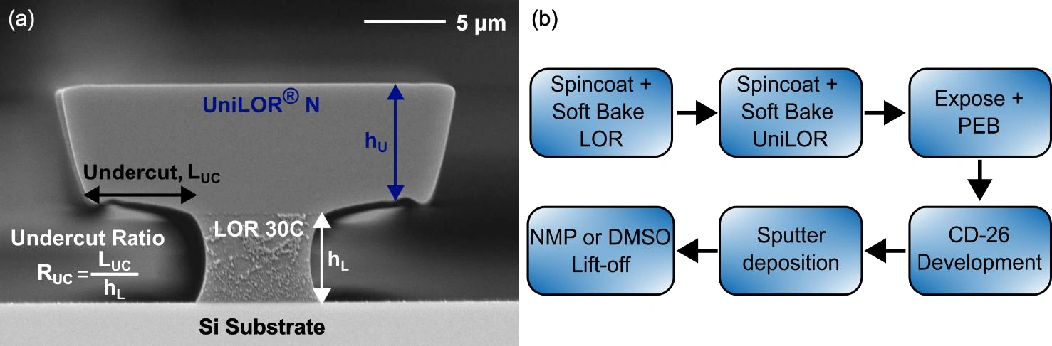
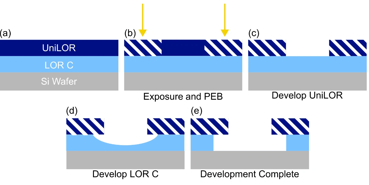
(a) Example lift-off bi-layer shape created by LOR 30C dilution and UniLOR® N 5.0 dilution with respective heights and undercut.
(b) Process flow for bi-layer lift-off process
- Higher Soft Bake Temperatures
- LOR C soft bake increased from 160°C → 200°C
- UniLOR® N soft bake increased from 115°C → 125°C
This reduced residual solvent and increased film density, prevents thermal deformation.
- Longer Development Times
Higher bake temperatures meant more robust films, requiring longer TMAH development to achieve desired undercuts leading to improved process control. - Tunable Undercut Geometry
They achieved stable undercut ratios of 1:1 to 2:1, ideal for optical filter stacks up to several microns thick.
While 3:1 is achievable, it can risk losing smaller features due to over‑development.
Key Data & Findings
- More Controlled Undercut Formation Higher bake temperatures significantly increased the development time needed to reach target undercuts—making the process more predictable and reducing variability.
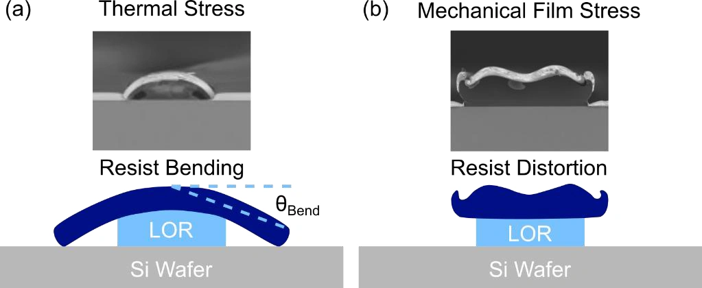
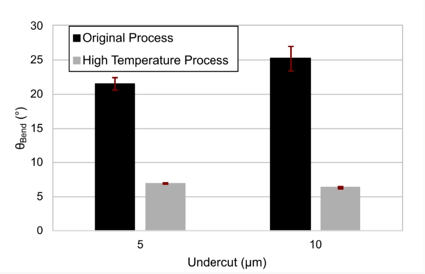
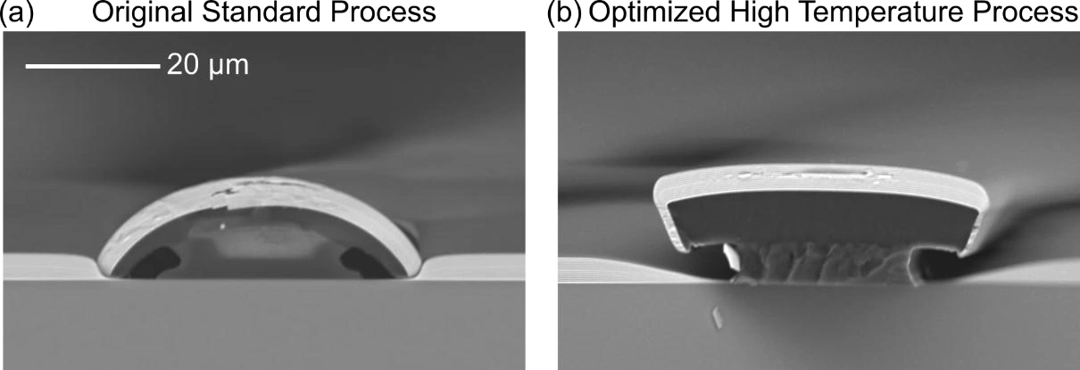
- Major Reduction in Resist Bending The team measured a “bend angle” (θ_bend) of the UniLOR® N layer after sputtering to quantify stress resistance.
- The optimized process reduced θ_bend by ~70% compared to the original process.
- This mechanical stability is critical to ensure the resist undercut remains open for the remover.
- This mechanical stability is critical to ensure the resist undercut remains open for the remover.
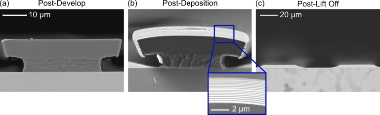
- Crisp pattern sidewalls
- Complete lift‑off with no fencing or bridging
- Stable structures even after deposition of multiple high‑stress metal oxide layers
What This Means for Optical Device Fabrication
With the optimized LOR C + UniLOR® N process, manufacturers can now:
- Pattern dielectric films requiring ≤180°C sputtering
- Reliably fabricate thick, multi‑layer optical filters
- Avoid etch‑related defects and material incompatibilities
- Scale up to advanced wafer‑level optics and photonic components
This opens the door for next-generation devices in:
- AR/VR waveguides
- Optical Sensors
- Interference filters
- Heterogeneous integrated photonics
- Wafer-level camera modules
Conclusion
The study shows that a carefully engineered bi‑layer lift‑off stack, paired with higher temperature processing, can fully withstand the harsh conditions of high temperature sputtering. The LOR C + UniLOR® N system not only survives these environments but delivers:
- Higher mechanical stability
- Cleaner lift‑off
- Greater process tuning range
As optical devices continue to grow in complexity and performance requirements, thermally robust lift‑off systems like this one will be foundational to next‑generation manufacturing.