Overview
SU-8 TF 6000 is a high-contrast, chemically amplified, negative tone epoxy-based photoresist designed for thin, highly uniform coatings. SU-8 TF 6000 can be used on a variety of substrates and has good adhesion to Si, SiN, SiO2, Glass, and Au. However, special processing is needed when using SU-8 TF 6000 on Au to avoid unwanted resist residue that occurs due to additional acid generation on this substrate. Au is an important material for device manufacturing due to its high conductivity and corrosion resistance, and this guide is provided as a method to ensure SU-8 TF 6000 can be used in gold-specific applications.
Please refer to the SU-8 TF 6000 Datasheet for additional information about the product series, cured material properties, and processing for other substrates.
Residue Description
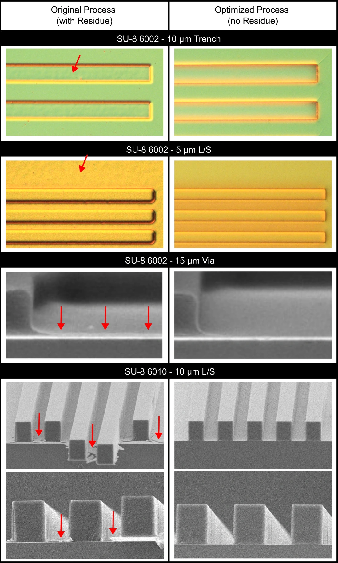
SU-8 TF 6000 exhibits resist residue when processed under standard TDS conditions on Au. This residue can be detected through Nomarski microscopy, SEM, and by testing electrical conductivity across open areas post-development using a multimeter as the residue prevents conductivity. The residue can present itself in a few ways:
- Non-exposed area exhibits a rough, textured surface
- Halo effect around features resulting in discoloration around features
- Roughness at the corners of via and trench features
To prevent this residue, an adjusted process was developed and compared to the original process. See Figure 1 for side-by-side images of the original and optimized process using both Nomarski microscopy and SEM across a variety of features and dilutions. For thinner dilutions, the residue is best seen using Nomarski microscopy as certain wavelengths highlight the thin, textured residue. For thicker dilutions, the residue can be readily observed either using SEM or Nomarski.
Key Process Changes
- O2 plasma surface treatment to create a thin oxide layer
- Lower soft bake temperature
- Lower PEB temperature
Optimized Process Conditions
To process SU-8 TF 6000 on Au, follow the recommended steps in Tables 1-2 as a baseline. For the baking steps, use of a level hotplate with good thermal control is recommended. Additionally, exposure dose may need to be adjusted depending on substrate type, film thickness, exposure tool, and filter. Exposure dose recommendations in Table 2 were selected based on sizing of 5 & 10 μm features. It is expected that a certain amount of optimization will be required for customer specific process equipment, facilities, substrates, and applications.
| Processing Conditions | |
|---|---|
| Wafer Pre-Treatment | Standard O2 plasma treatment Example conditions: 40 sccm, 100W, 3 min |
| Coat | Dispense 1 mL/inch of substrate 1000-4000 rpm for 30 sec |
| Soft Bake | 75°C using times in Table 2 |
| Exposure | i-, h-, or g-line using exposure doses in Table 2 Verify intensity for your specific tool and filter set-up |
| Post Exposure Bake | 75°C using times in Table 2 |
| Development | 3 min in SU-8 Developer Recommendation is to use spray-puddle method with three puddles. |
| Hard Bake (optional) | 150-200°C for 30-60 minutes |
Table 1. SU-8 TF 6000 Recommended Processing on Au
| DILUTION | SOFT BAKE TIME minutes @ 75°C |
EXPOSURE ENERGY mJ/cm2 |
PEB minutes @ 75°C |
|---|---|---|---|
| 6000.5, 6001 | 2 | 80-100 | 2 |
| 6002 | 3 | 80-100 | 2 |
| 6005 | 5 | 100-120 | 4 |
| 6010 | 10 | 100-120 | 4 |
Table 2. Bake times and exposure doses for various SU-8 TF 6000 dilutions
Industrial Relevance
Au is often used in microelectronics due to its distinct material properties such as high conductivity, optical reflection, corrosion resistance, and biocompatibility. [1] As such, Au is a preferred material for contacts and wire bonding required to route electrical signals. Au electrodes can also be integrated into microfluidic devices for lab-on-a-chip or biosensing/sorting applications. [2-3]
Given that SU-8 is commonly used as a permanent structure in device fabrication, it is critical that SU-8 TF 6000 is compatible with a variety of substrates, including Au. [4-5] The process described here can be used to ensure SU-8 TF 6000 patterning on Au does not disrupt the critical electrical conductivity between Au and the rest of the device.
References
[1] T. A. Green, Gold Bulletin, 40, 105-114 (2007). doi.org/10.1007/BF03215566
[2] K. Mutafopulos et al. Lab on a Chip, 20, 3914-3921 (2020). doi.org/10.1039/D0LC00723D
[3] S. Mahmud and D. Dutta, Analytical Letters, 57, 2927-2941 (2023). doi.org/10.1080/00032719.2024.2307458
[4] M. Nordstrom et. al. Microelectronic Engineering, 78-79 (2005). doi.org/10.1016/j.mee.2004.12.021
[5] A. Ezkerra et. al. J. Micromech. Microeng. 17, 2264-2271 (2007). doi:10.1088/0960-1317/17/11/013