Explore how our materials support your
process, from microfluidics to wafer bonding.
Creates durable thick-film molds for clean, precise metal deposition. Maintains definition through long plating cycles.
Enables accurate metal buildup with high aspect ratios. Provides stable resist molds for uniform electroplating.
Creates durable thick-film molds for clean, precise metal deposition. Maintains definition through long plating cycles.
Lift-off resists enable the patterning of difficult to etch noble metals
T‑gates provide a low‑resistance, self‑aligned gate structure ideal for high‑frequency III–V transistor fabrication.
Demonstrated capability for plating molds for micro-gear structures
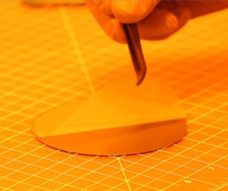
Enables Soft-lithographic mold creation for the prototyping of microfluidic chip designs.
Creation of robust array structures for material sequencing.
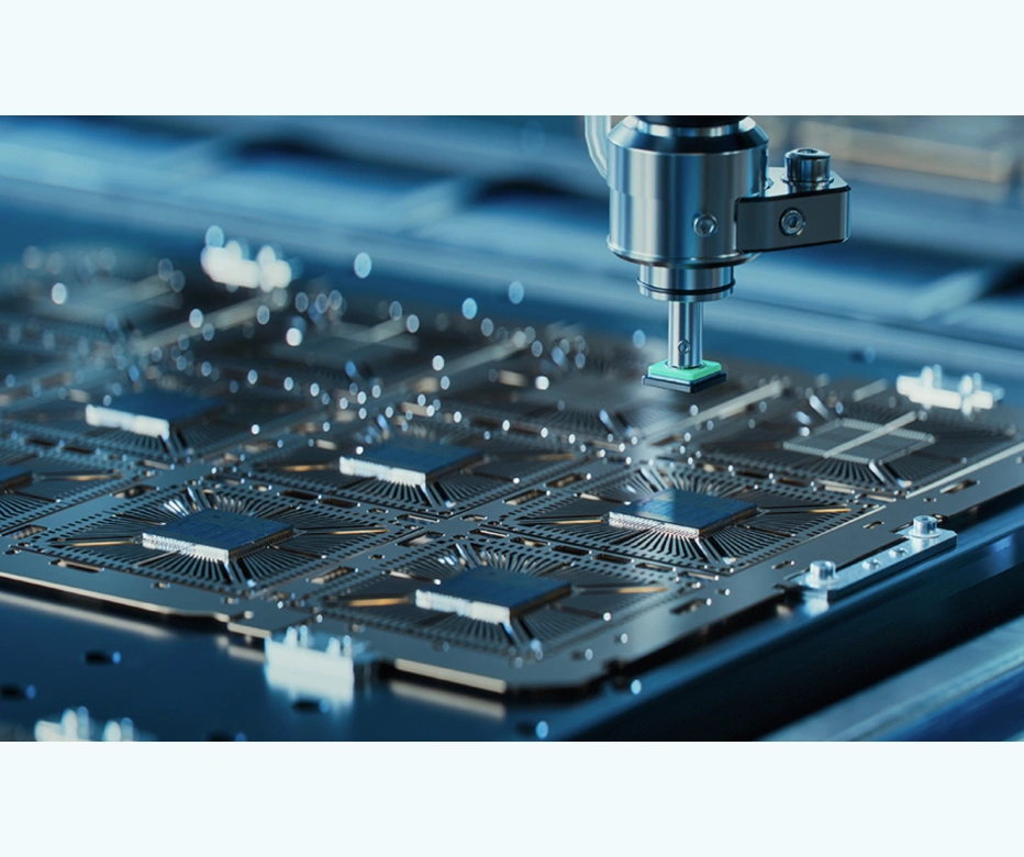
Wafer bonding enables the integration of dissimilar materials and device layers through direct joining of separately fabricated wafers.
Microfluidics enables precise manipulation of small fluid volumes within microscale channels for controlled chemical and biological processing.
Enables deposition patterning of difficult to etch materials such as Nobel metals and metal-oxides.