Overview
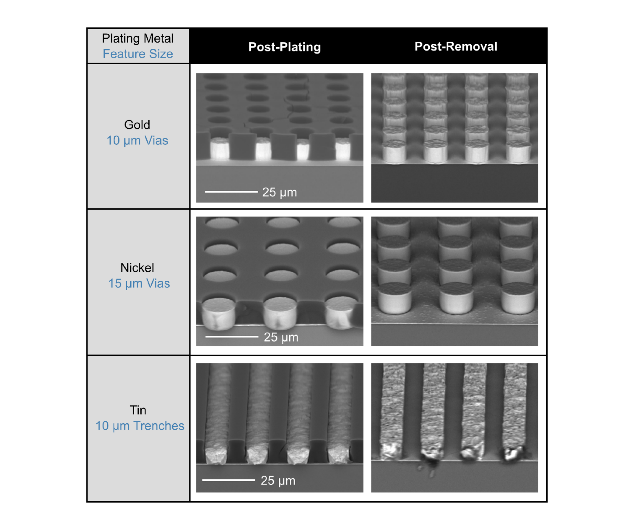
TempKoat® N50 is a chemically amplified, negative-tone resist series for advanced packaging and MEMS applications. It is ideally suited for electroplating as it can be easily removed post-plating to pattern metals such as Cu, Ni, Sn, and Au up to 100 μm. TempKoat® N50 is an upgraded TempKoat® N product that offers a wider thickness range, PFAS/PFOS free formulation, and excellent aspect ratio for thick plating requirements.
Contact Kayaku Advanced Materials for more information about the formulations highlighted here.
Application
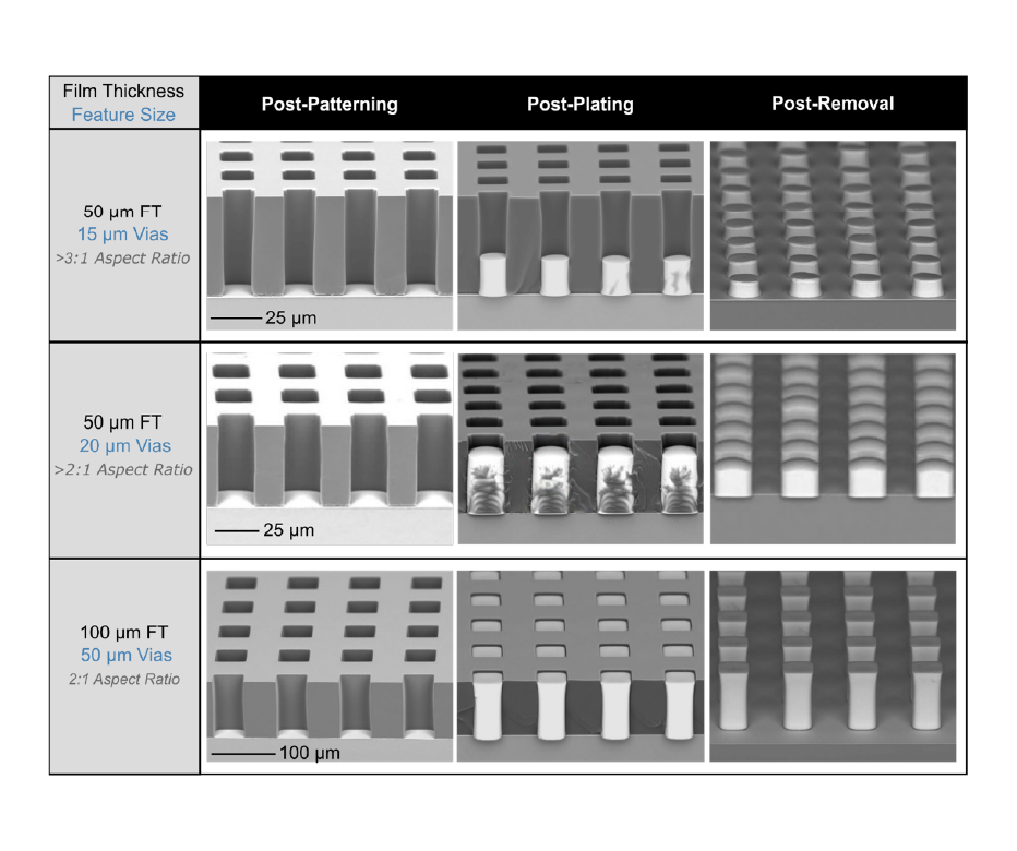
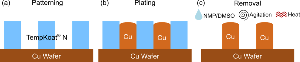
TempKoat® N50 is an advanced, temporary plating material that enables thick, high aspect ratio plated features to meet the increasing demands of packaging and integration. For a successful plating process, the resist needs to produce sharp feature profiles, withstand plating chemistries, and be cleanly removed postplating (Figure 1). TempKoat® N50 fulfills these requirements thus enabling applications in wafer level packaging such as redistribution layers and copper bump plating. The high aspect ratio achieved by TempKoat® N50 (>3:1) is also crucial to 3D integration using tall, tightly spaced interconnects which have become increasingly important for advanced device architectures. Importantly, to sustain environmental compliance and process security the resist was also formulated to be NMP and PFAS/PFOS free.
Key Features
- Negative tone, chemically amplified resist
- PFAS/PFOS free formulation
- 20-75 μm film thickness (single coat)
- i-Line/Broadband sensitivity
- Excellent resistance to copper, nickel, tin, and gold plating chemistries
- Residue-free removal
Process Conditions
(a) Patterning
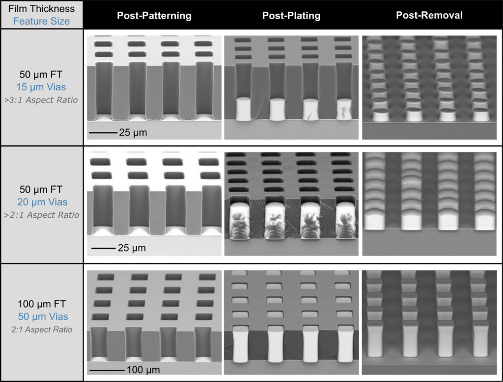
TempKoat® N50 can be used to coat film thicknesses from 20-75 μm in a single coat and >100 μm using a double coat. Here, we highlight processes for 50 and 100 μm film thicknesses (FT) to capture a variety of metal patterning needs. See Table 1 for detailed process steps for patterning at these thicknesses.
For the baking steps, use of a level hotplate with good thermal control is recommended. Additionally, exposure dose may need to be adjusted depending on substrate type, film thickness, exposure tool, and filter. It is expected that a certain amount of optimization will be required for customer specific systems, facilities, substrates, and applications.
| Step | 50 µm FT (Single Layer) | 100 µm FT (2 Layers) |
|---|---|---|
| Coat | Dispense 1 mL/inch of substrate 1000-4000 rpm for 30 sec | |
| Soft Bake | 2 min @ 65°C 20 min @ 105°C | 1st Layer: 3 min @ 65°C, 15 min @ 110°C2nd Layer: 15 min @ 110°C |
| Exposure (365 nm) | 300-500 mJ/cm2 Verify dose for your specific tool and filter set-up. | |
| Post-Exposure Bake | 10 min @ 90°C | 3 min @ 65°C 10 min @ 95°C |
| Development | 9 min with TMAH Developer | 13 min with TMAH Developer |
Table 1. Typical processing conditions for patterning of 50 and 100 μm films
(b) Plating
Plating conditions vary by desired metal and may need to be optimized for your specific plating equipment. See Table 2 for typical conditions using Technic tools and chemicals.
| Metal | Plating Solution | pH | Temperature | Current Density (ASF) |
|---|---|---|---|---|
| Copper | Elevate Copper 6388 | <1 | 25°C | 25 |
| Nickel | Elevate Nickel 5950 | 4.5-4.9 | 25°C | 20 |
| Tin | Elevate Tin D5011 | <0.5 | 25°C | 20 |
| Gold | Elevate Gold 7934 | 5.8-6.4 | 50°C | 3 |
Table 2. Typical plating conditions for Cu, Ni, Sn, and Au
(c) Removal
As TempKoat® N50 is formulated to be a temporary resist, it is completely soluble in organic solvents. For effective and clean resist removal, submerge wafers in resist stripping tank using recommended conditions in Table 3 below. Importantly, TempKoat® N50 can withstand long plating times, up to 2 hours, with stable material performance.
| Stripping Chemical | Remover PG (Kayaku Advanced Materials), INTERVIA™ 2011 (Qnity), or NK Poleve 480 (NKC) |
| Agitation | Agitated immersion or ultrasonics |
| Heat | 50-80°C |
Plating and Removal Results
Films processed using the above conditions were imaged post-patterning, post-plating, and post-removal to demonstrate the successful metal patterning capabilities using Cu (Figure 2). These processes can be adapted to various feature shapes, thicknesses, and plating metals as needed for your individual application.
Industrial Relevance
Recent evolution in chip integration technologies continues to drive the need for advancement in plating and etch capabilities. In particular, the rise of advanced packaging solutions such as fan out wafer level packaging (FOWLP) and 3D packaging is intensifying requirements for thicker copper features with high aspect ratios. [1-2] These copper features enable vertical interconnects and reduced layer counts for cost effective scaling which is crucial for chiplet and memory on logic architectures. [3-4] Meeting these demands requires lithography materials that combine thickness capability, sharp profile control, and compatibility with widely available exposure tools. TempKoat® N50 was formulated to meet these demands and enable next-generation plating solutions for relevant sectors such as artificial intelligence, high performance computing, and 5G technologies.
References
[1] J. H. Lau, IEEE Transactions on Components, Packaging and Manufacturing Technology, 12, 2, 228-252, (2022). doi: 10.1109/TCPMT.2022.3144461
[2] K. Best et al. IMAPS Proceedings 2015, 000793-000798. (2015).
https://doi.org/10.4071/isom-2015-THP23
[3] W. Koh, B. Lin and J. Tai, International Conference on Electronic Packaging Technology and High Density Packaging, 1-5, (2011). doi: 10.1109/ICEPT.2011.6067027.
[4] E. J. Marinissen et. al. Handbook of 3D Integration: Design, Test, and Thermal Management, Volume 4, Chapter 12, (2019). https://doi.org/10.1002/9783527697052.ch12
Downloads