Overview
TempKoat® P is a chemically amplified, positive tone, temporary resist formulated for advanced packaging and MEMS applications. Specifically, TempKoat® P is capable of producing high aspect ratio features from thick, single coatings. The unique combination of resolution, excellent chemical resistance, and residue-free removal make it ideal for critical electroplating applications.
Application
TempKoat® P is a versatile resist used for plating applications spanning RDL, wafer bump, and beyond. Plating is an electrochemical deposition method with the following steps in Figure 1.
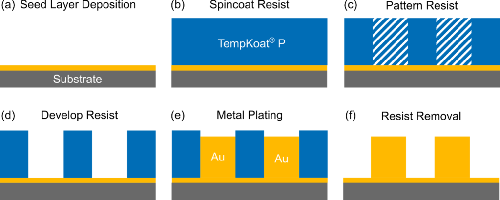
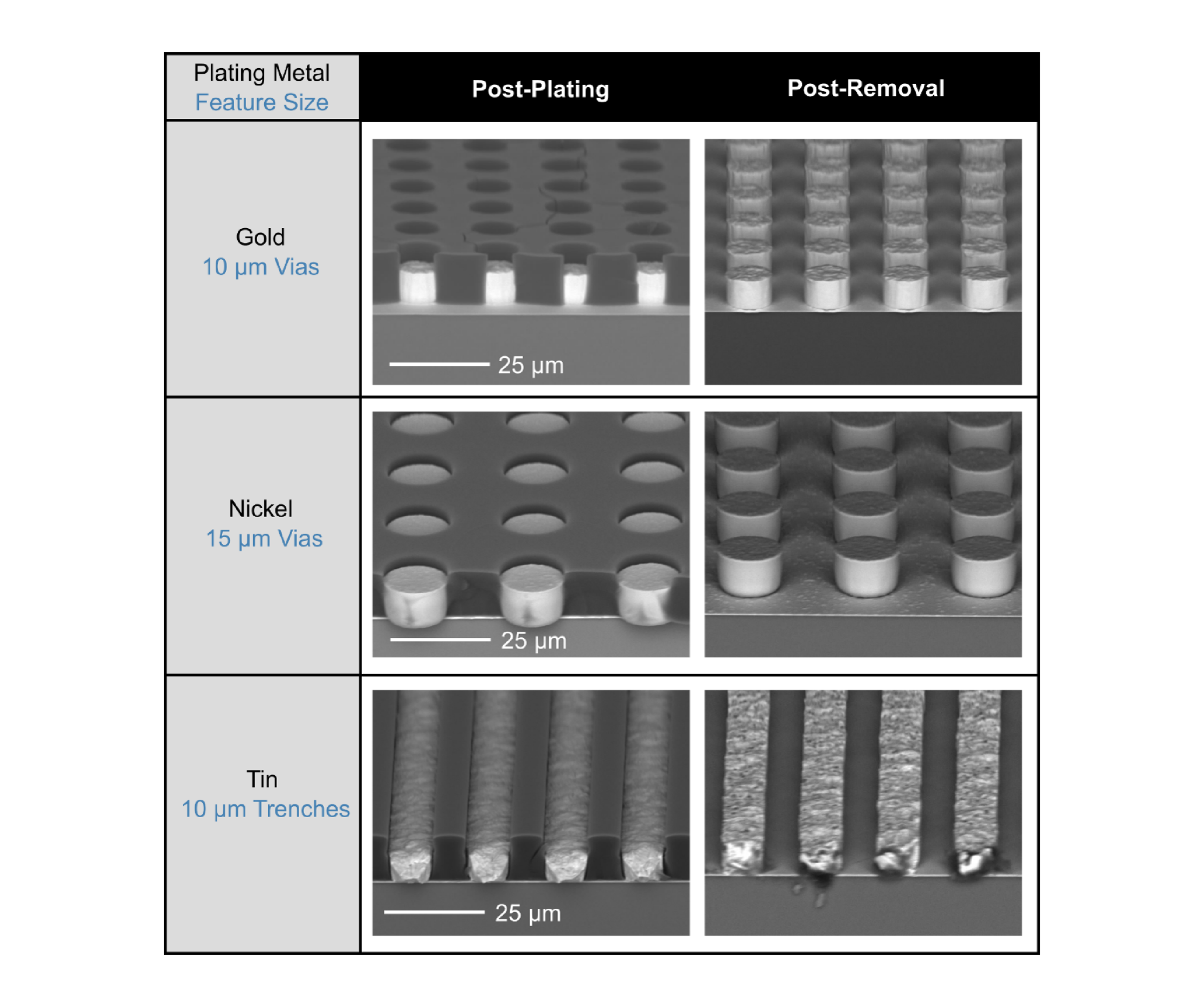
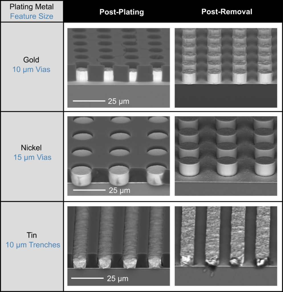
This method enables clean, targeted fabrication of metal features without the need to etch back unwanted material. The deposition of different kinds of metals necessitates the photoresist to withstand a wide range of harsh chemical environments. TempKoat® P is compatible with various plating media including, but not limited to copper, gold, nickel, tin, and more. This note highlights TempKoat® P’s compatibility with Au, Ni, and Sn, specifically Technic’s Elevate® Au 7934, Elevate® Ni 5950, and Elevate® Tin D5011. For more information on Cu plating, see the TempKoat® P Technical Data Sheet.
Key Features
- Broad film thickness range
- 3:1 height-to-width aspect ratio
- Fine pattern fidelity and reliability
- No rehydration delay or latency post exposure
- Excellent chemical resistance
- Compatible with various plating media
- Easy removal
Processing Guidelines
| Processing Guidelines for Ni and Sn | |
|---|---|
| Coat | Dispense 1 mL/inch of substrate Spin at 3,000 rpm for 30 sec |
| Soft Bake | 3 min @ 120°C |
| Exposure | 350 mJ/cm² (at 365 nm) Verify dose for your specific tool and filter set-up |
| Post Exposure Bake | 2 min @ 120°C |
| Development | 4x 60s puddles with TMAH Developer |
| Plating pre-treatment | Rinse with DI Water 2 minutes in Elevate Cu 6300 Cleaner – 90°F (23°C) • 15% v/v in DI Water Rinse with DI Water 1 minute in Sulfuric Acid 10% Rinse with DI Water |
| Processing Guidelines for Au | |
|---|---|
| Coat | Dispense 1 mL/inch of substrate Spin at 3,000 rpm for 30 sec |
| Soft Bake | 3 min @ 120°C |
| Exposure | 150 mJ/cm² (at 365 nm) Verify dose for your specific tool and filter set-up |
| Post Exposure Bake | 2 min @ 95°C |
| Development | 4x 60s puddles with TMAH Developer |
| Plating pre-treatment | Rinse with DI Water 2 minutes in Elevate Cu 6300 Cleaner – 90°F (23°C) • 15% v/v in DI Water Rinse with DI Water 1 minute in Sulfuric Acid 10% Rinse with DI Water |
| Metal | Plating Solution | pH | Temperature | Current Density (ASF) | Time (min) |
|---|---|---|---|---|---|
| Gold | Elevate® Gold 7934 | 5.8 – 6.4 | 122°F (50°C) | 3 | 30 |
| Nickel | Elevate® Nickle 5950 | 4.5 – 4.9 | 125°F (52°C) | 20 | 13 |
| Tin | Elevate® Tin D5011 | < 0.5 | 77°F (25°C) | 20 | 6.5 |
| Solution | Temperature (°C) | Time (hr) | Extractables |
|---|---|---|---|
| Elevate Gold 7934 | 50 | 24 | Below Detection |
| Elevate Ni 5950 | 52 | 24 | Below Detection |
| Elevate Tin D5011 | 25 | 24 | Below Detection |
Industrial Relevance
Gold, nickel and tin are among the most prevalent finishes throughout the semiconductor industry, each one valued for different properties. Electroplated gold has high conductivity and mechanical wear resistance making it very useful for wire bonding, connectors and switches.[2] Nickel on the other hand is valued for its ability to act as a barrier between different device layers through extreme temperature swings.[1] Lastly, Tin has strong anti-corrosive properties as well as high electrical conductivity and solderability which make it ideal for making highly reliable electrical connections.[3]
Importantly, each metal requires a different plating media which typically contain harsh chemistries. The often cyanide-based plating media of gold has a strong affinity for gold ions which limits the speed of plating and necessitates long plating times.[4] Nickel plating media must be tightly controlled and free of contamination to control the stress, purity and reliability of the deposition. Tin plating media is often extremely acidic with pHs below 1. These difficult conditions require a plating resist that can withstand harsh environments without degrading, deforming, or delaminating. TempKoat® P is shown to be a robust resist when exposed to various plating media and enables these critical metallization processes for semiconductors, MEMs, and other devices.
References
[1] E. Shalyt et. al. ECS Meeting Abstracts, MA2014-02 1714, (2014). DOI 10.1149/MA2014-02/33/1714
[2] Y. Okinaka and M. Hoshino, Gold Bulletin, 31, 3-13 (1998) https://doi.org/10.1007/BF03215469
[3] Noble Metal Coatings Inc, Primary Applications of Tin Electroplating in Electronics, (2024).
[4] R. Morrissey, Technic Inc. Gold and Silver Plating Basics, Products Finishing, (2011).