Overview
UniLOR® N is a negative-tone, chemically amplified proprietary co-polymer resist for use in UV lithography for semiconductors, MEMS and other nanofabricated structures. It is ideally suited for lift-off applications due to easy removal with commonly used resist strippers (NMP, DMSO). For certain deposition processes, high thermal stability of the resist is critical. This guide provides information on UniLOR® N’s thermal stability across a variety of temperatures for both single layer and bi-layer applications, along with a detailed look at an optical filter patterning application. Please refer to the UniLOR® N Datasheet for more information about the material’s properties, available dilutions, and tunability.
Application
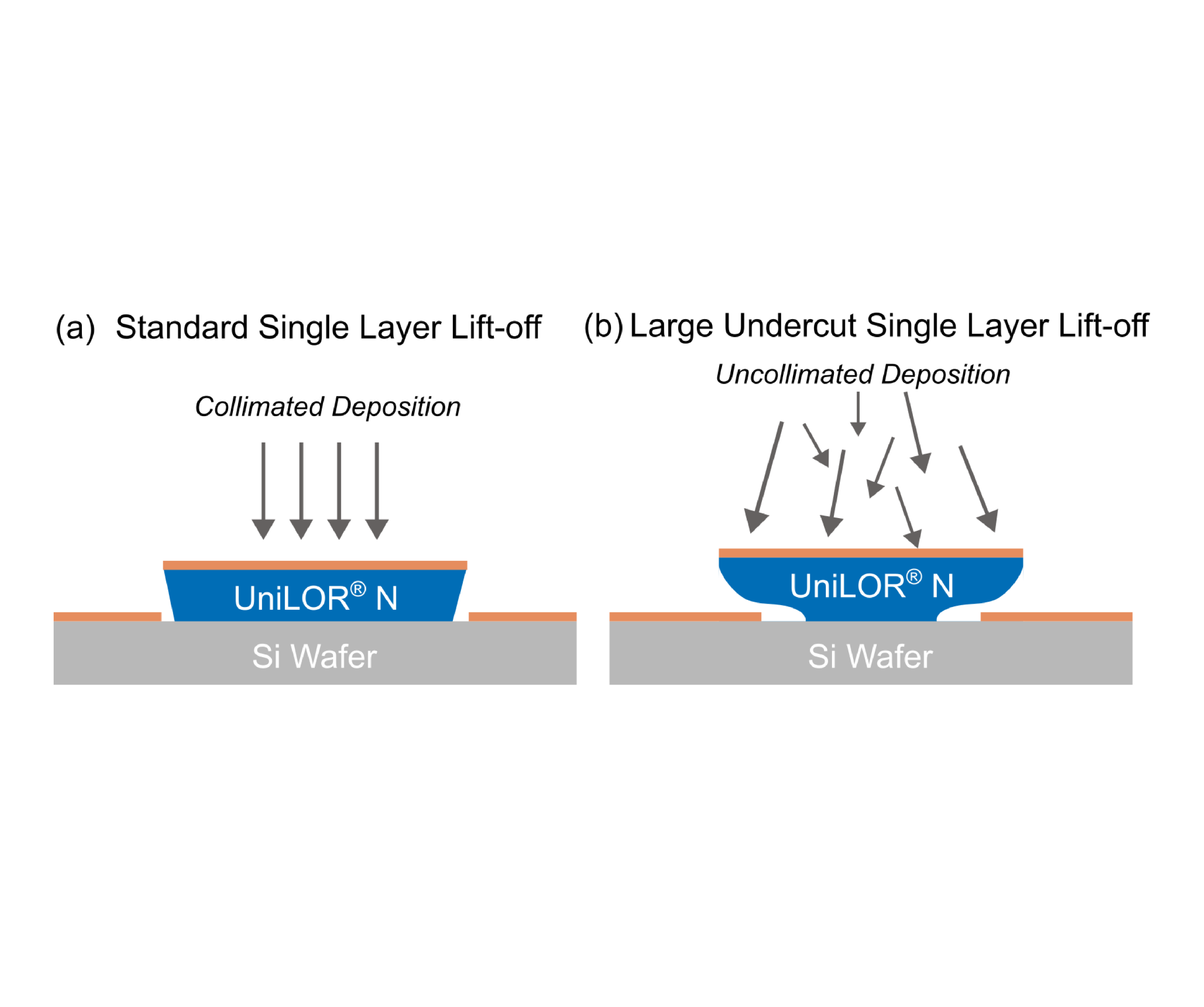
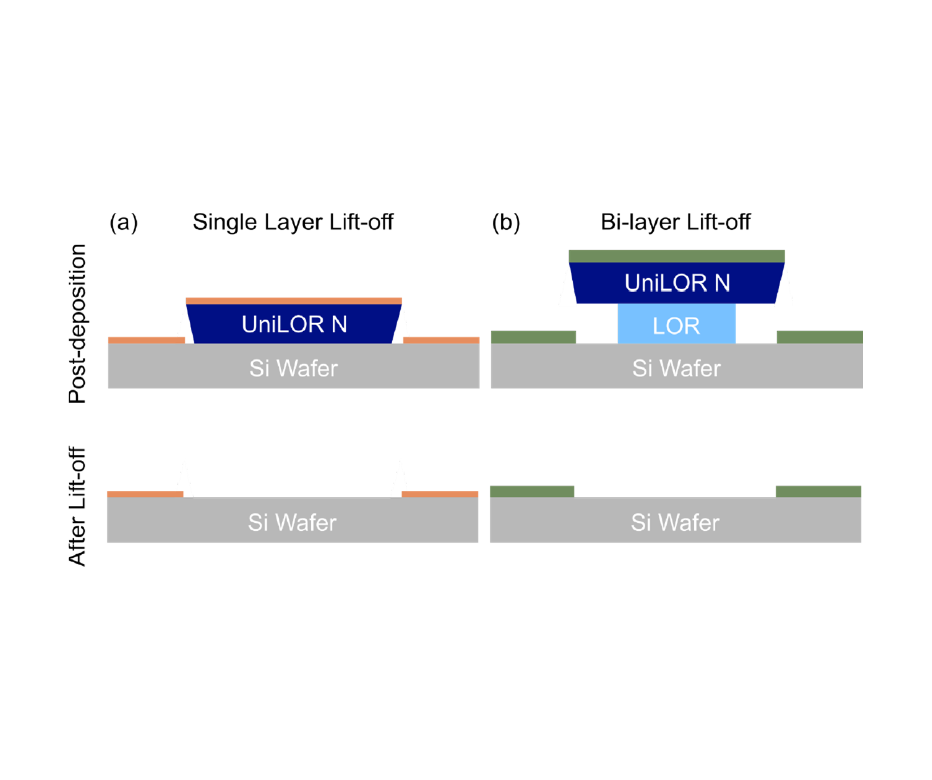
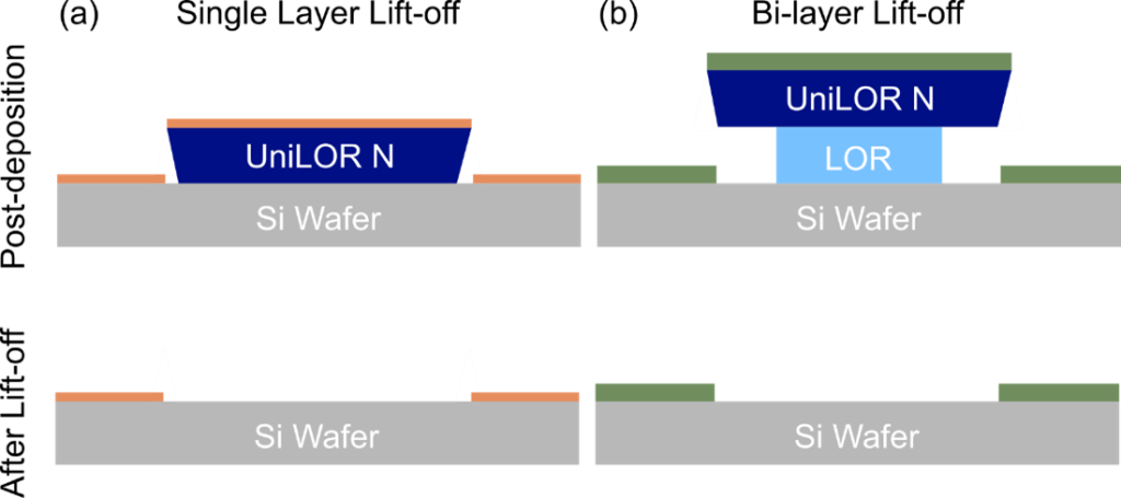
UniLOR® N is a versatile resist used for lift-off applications spanning imaging, sensing, and photonic devices. Lift-off is a microfabrication technique in which a sacrificial photoresist layer is first patterned on the substrate, then a target material is deposited over the entire surface, and finally the material deposited over this resist stack can be selectively removed by dissolving the resist. This method enables clean definition of metal or dielectric features when etching is not a viable option. Single layer lift-off is appropriate for directional metallization processes whereas the bi-layer architecture is more suitable for lift-off of thicker dielectric or metal oxide materials deposited using methods such as sputtering. Figure 1 illustrates the difference between the two lift-off architectures.
Key Features
- Tunable sidewall profile angle
- Ideal for both single layer and bi-layer lift-off processes
- Thermal resistance for geometric stability in deposition at elevated temperatures
- Compatible with many substrates (Si, Cu, GaAs, SiC)
Process Conditions & Stability – Single Layer
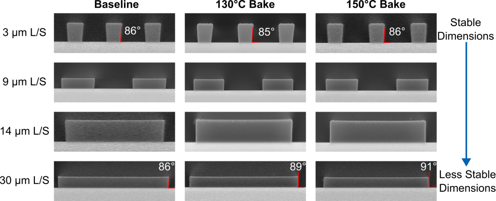
For evaluating thermal stability as bake temperature increases, films were processed using conditions in Table 1 and several Line/Space (L/S) features were imaged.
| Processing Conditions & Stability – Single Layer | |
|---|---|
| Coat | Dispense 1 mL/inch of HMDS-primed Si substrate 1000-4000 rpm for 30 sec |
| Soft Bake | 2 min @ 115°C |
| Exposure | 120-200 mJ/cm² (at 365 nm) Verify intensity for your specific tool and filter set-up. |
| Post Exposure Bake | 2 min @120°C |
| Development | 45 sec with TMAH Developer |
| Hard Bake Conditions | None, 130°C, and 150°C for 30 min |
Table 1. Process conditions using UniLOR® N 2.5 dilution with variable hard bakes
After processing UniLOR® N 2.5 per standard conditions, features were subjected to high temperature bakes at 130°C and 150°C. Images from 3, 9, 14, and 30 μm features are shown in Figure 2. Importantly, the sidewall angle of the single layer process is critical to enabling lift-off. Sidewall angles were quantified as a measure of dimensional stability and are indicated in Figure 2. Smaller features are stable up to 150°C. Larger features are less stable and exhibit worsening sidewall angle as temperature increases. This observed phenomenon can be attributed to the surface area to volume ratio specific to any given feature size. As such, smaller features are better suited for lift-off if high temperatures are required.
Process Conditions & Stability – Bi-layer with LOR
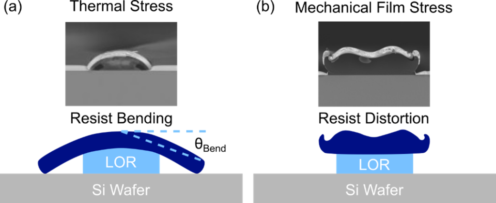
For bi-layer lift-off, the structural integrity of the T-shape resist feature is crucial to successful lift-off. When exposed to elevated temperatures (≤180°C), standard resists undergo softening or glass-transition-driven flow as seen in Figure 3(a) which causes the resist to bend by angle θBend. Some sputtering applications require deposition of high stress, multi-layered materials that can cause resist distortions like those in Figure 3(b).
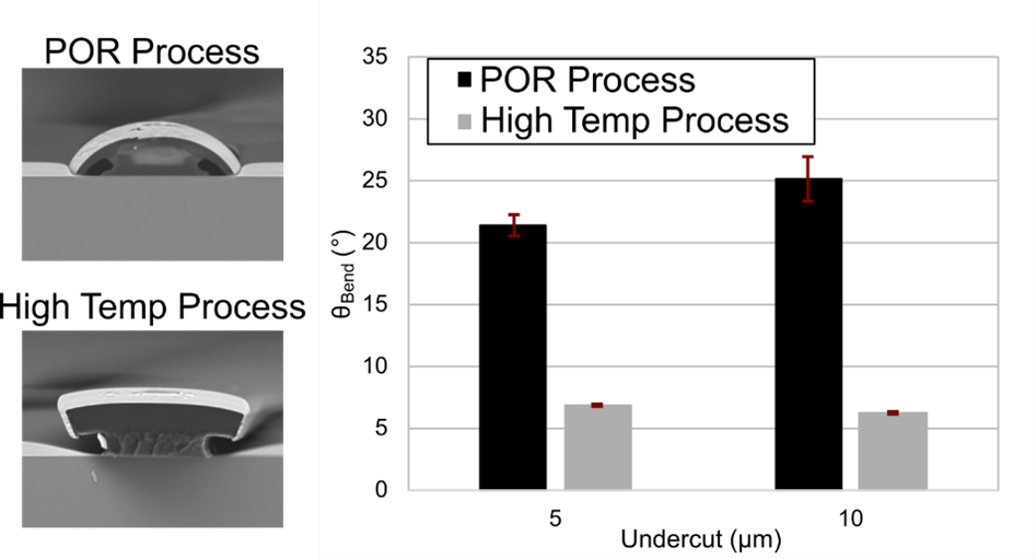
To address this issue, a high temperature process was developed using UniLOR® N which greatly reduced the effects of thermal and mechanical stress up to 180°C. Notably, the resist angle was quantified in Figure 4 and improved by ~70% using the high temperature process in Table 2. Note that development time is a variable in this technique and should be tuned for the user’s application. A 1:1-2:1 ratio of undercut length to LOR height was appropriate for most cases and can serve as a starting point. See the LOR/PMGI Datasheet for more information about available LOR product offerings.
| Processing Conditions for Stability Study – Optimized for High Temperature | |
|---|---|
| Coat LOR 30C | Dispense 1 mL/inch of substrate 1000-4000 rpm for 30 sec |
| Soft Bake LOR 30C | 3 min @ 65°C 5 min @ 200°C |
| Coat UniLOR® N | Dispense 1 mL/inch of substrate 1000-4000 rpm for 30 sec |
| Soft Bake UniLOR® N | 3 min @ 125°C |
| Exposure | 400-600 mJ/cm² (at 365 nm) Verify dose for your specific tool and filter set-up. |
| Post Exposure Bake | 4 min @ 120°C |
| Development | TMAH-based developer Typical times from 150-400 sec, but will depend on desired undercut. |
| Deposition | Deposit desired metal or dielectric material in chamber ≤180°C |
| Lift-Off | 30 min in NMP or DMSO-based remover @ 50°C Rinse with fresh remover and dry with N2 |
Table 2. Bi-layer process conditions using LOR C and UniLOR® N for high temperature applications
Industrial Relevance
High-performance optics applications require dielectric films that are dense, low absorption, and stoichiometrically stable. These films are commonly made of metal oxides such as SiO2, TiO2, Al2O5, and Nb2O5 which require high temperature sputtering to achieve the desired stoichiometry and controlled refractive index. Typical deposition temperatures in advanced sputtering tools, including the Bühler Leybold Optics HELIOS 800 system used here, [1] range from 150 °C to >180 °C depending on the coating design and target material. To pattern materials deposited in this temperature range, robust lift-off resist materials such as UniLOR® N are needed. By using the high temperature process described here, optical filters sputtered using the HELIOS 800 system were successfully lifted without fencing, flagging or other typical lift-off defects. [2-4] A series of SEMs taken throughout the bi-layer lift-off process of optical grade materials are included in Figure 4 to highlight the LOR C + UniLOR® N system. For more information on this optical filter application, see reference [5]. This method can be tuned for a variety of applications and lift-off materials by adjusting the T shape and process conditions. Please contact Kayaku Advanced Materials if you need guidance for your specific application.
References
[1] J. Lumeau et. al. Optical Interference Coatings Conference, Technical Digest Series, (2025). https://doi.org/10.1364/OIC.2025.WE.4
[2] A. Elshenety et al. Journal of Micromechanics and Microengineering, 35, 025012 (2025). https://doi.org/10.1088/1361-6439/adac6b
[3] A. Fuchs et al. Solid State Phenomena, 359, 71-77 (2024). https://doi.org/10.4028/p-i1Arj1
[4] K. Cheng, IEEE Transactions on Semiconductor Manufacturing, 33, 564-568 (2020). 10.1109/TSM.2020.3008604
[5] A. Rendos et al. Proc. of SPIE, 13899, (2026). doi: 10.1117/12.3079850