Overview
PermiNex® 1000 and 2000 are epoxy‑based, photo‑imageable bonding resists engineered for high precision adhesive layers in advanced device and wafer-level packaging. Designed for cavity definition and wafer bonding in applications such as BAW, SAW, and microfluidic devices, these resists provide excellent alignment accuracy, low temperature processing, and high-quality bond formation. PermiNex® adhesives enable patterning and bonding of substrates while maintaining high bond integrity, fine feature definition, and robust adhesion at processing temperatures below 200°C.
The key distinction between the two series is the development process. The PermiNex® 2000 series formulation was developed for aqueous development in TMAH, making it suitable for process environments where aqueous development is preferred. Due to the aqueous development process, PermiNex® 2000 series incorporate a post-develop bake (PDB) to remove residual water prior to bonding. The PermiNex® 1000 series is developed in the PN 1000 developer, which is a solvent blend.
This application note describes PermiNex® 1000 and 2000 selection recommendations based on substrate compatibility, development process, and application requirements. For additional assistance selecting the appropriate PermiNex® material for your bonding process, please contact Kayaku Advanced Materials.
Application
The PermiNex® series is ideal for bonding in microelectronic and microfluidic manufacturing and packaging applications where structural integrity and process flexibility are important. It is used as a photo-imageable adhesive for wafer bonding in BAW, SAW, lab-on-a-chip (LoC), and other microfluidic devices. These applications can incorporate myriad substrate materials, including Si, metals, glass, and specialty materials like GaAs and LiNbO3.
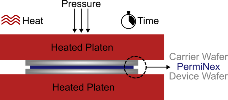
A successful bonding process requires application of heat and pressure to the two substrates after patterning the PermiNex® material as shown in Figure 1. Bonding parameters should be optimized based on factors such as substrate materials, substrate size, device geometry, and process requirements.
Key Features
- Negative tone, photo-imageable adhesives
- Alkaline (PermiNex® 2000) and solvent (PermiNex® 1000) developable series
- High resolution patterning
- Low temperature processing (< 200°C)
- High quality, void-free bonding
- Superb adhesion to silicon and glass
- Good process compatibility (dicing, soldering) and high reliability (HAST, TCT)
Processing Information
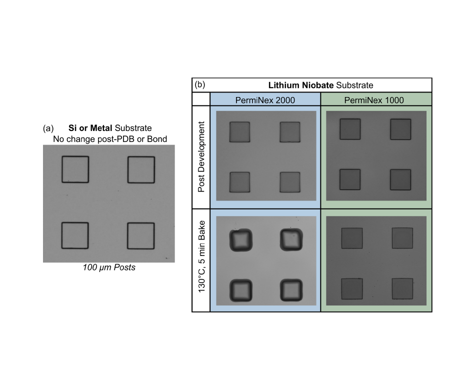
Typical substrates for photo-patternable bonding are Si and glass, but as device complexity increases, multi-substrate or unique substrate devices are becoming more popular. Substrates such as Si, SiN, and metals including Au can generally be processed using conditions similar to those provided in the standard Perminex® data sheets. However, glassy and specialty substrates may require additional process optimization. For example, Lithium Niobate is a common material for SAW devices due to its piezoelectric properties. To evaluate PermiNex® material selection for Lithium Niobate substrates, the lithographic performance of the PermiNex® 1000 and 2000 series was compared.
With PermiNex® 2000, the Lithium Niobate substrate quenched the photochemical reaction, thus leading the resist to reflow during the post development bake at 130°C. In contrast, the PermiNex® 1000 series did not exhibit the same quenching effect, and patterned features remained stable at elevated temperatures (Figure 2b). Where aqueous development is required, the spreading observed with PermiNex® 2000 may be mitigated through process adjustments such as a post-development flood exposure and/or an extended PEB.
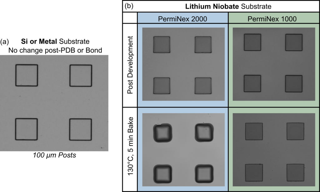
For starting process conditions on Lithium Niobate with PermiNex® 1000, see Table 1. Note that Lithium Niobate can exhibit the pyroelectric effect when quickly heated, so ramped baking and cooling may be required.
| PermiNex® 1000 — Processing Conditions | |
|---|---|
| Resist | PermiNex® 1000 |
| Thickness | 2 µm |
| Soft Bake | 6 min @ 95°C |
| Exposure | 2 J |
| PEB | 2 min @ 70°C |
| Development | PN1000, 1–2 min |
| PDB | N/A |
Table 1. Recommended starting process conditions for PermiNex® 1000 on Lithium Niobate substrates. After processing, substrates should be bonded and then cured at 180°C for 1hr.
For glass substrates, resist adhesion is a common issue and affects applications in displays, microfluidics, MEMS, and other optics devices. If coating on glass, certain process changes should be implemented for the best patterning performance of PermiNex®. Glass substrates typically require a longer soft bake and higher exposure dose. Starting process conditions on glass substrates are provided in Table 2.
| PermiNex® 1000 vs. 2000 — Processing Conditions for Glass Substrates | ||
|---|---|---|
| Resist | PermiNex® 1000 | PermiNex® 2000 |
| Thickness | 5 µm | 5 µm |
| Soft Bake | 12 min @ 95°C | 16 min @ 95°C |
| Exposure | 1.5 J | 1.2–1.5 J |
| PEB | 2 min @ 70°C | 6 min @ 70°C |
| Development | PN1000, 1–2 min | CD-26, 90 sec |
| PDB | N/A | 5 min @ 130°C |
Table 2. Recommended starting process conditions for PermiNex® on glass substrates. After processing, substrates should be bonded and then cured at 180°C for 1hr.
While glass and Lithium Niobate are commonly used with PermiNex®, other applications may introduce unique restrictions. For example, Al substrates are readily etched by TMAH-based developers, so PermiNex® 1000 series is recommended for applications incorporating Al. A selection guide is included in Table 3, but for specific recommendations for your application or device, please contact Kayaku Advanced Materials.
| Substrate | Typical PermiNex® Series Recommendation |
|---|---|
| Si | PermiNex® 1000 or 2000 |
| Au | PermiNex® 1000 or 2000 |
| Al | PermiNex® 1000 |
| Glass | PermiNex® 1000 or 2000, *note Table 2 |
| Lithium Niobate | PermiNex® 1000 |
Table 3. Typical PermiNex® series recommendations for various common substrate types
Industrial Relevance
The continued growth of RF, MEMS, and microfluidic technologies is increasing the need for wafer-level packaging and bonding processes that can accommodate diverse substrate materials while maintaining precise pattern definition and reliable bond formation. In RF front-end devices, surface acoustic wave (SAW) and other acoustic filters are important components for frequency selection in wireless communication systems. Newer acoustic resonator technologies are being developed for broader bandwidths and higher frequency 5G and future 6G applications. [1-2] Lithium Niobate is particularly relevant to these applications because of its piezoelectric properties and use in SAW device fabrication. [1]
Substrate and bonding considerations are important in microfluidic and lab-on-a-chip (LoC) devices, where patterned bonding layers are used to create enclosed channels, chambers, and fluidic structures. These platforms support applications including point-of-care diagnostics, biosensing, sample analysis, and organ-on-a-chip systems for biomedical research and drug development. [3-5] As these devices increasingly integrate silicon, glass, metals, and specialty substrates such as Lithium Niobate, material selection and substrate compatibility become important considerations for reliable photo-patternable bonding. The PermiNex® 1000 and 2000 series provide complementary processing options that allow bonding-material selection based on substrate and development requirements.
References
[1] J. Mei, N. Zhang, J. Friend, J. Vis. Exp. 160, (2020), e61013. doi:10.3791/61013
[2] G. Giribaldi, L. Colombo, P. Simeoni, M. Rinaldi, Nat. Commun. 15, 304, (2024). doi:10.1038/s41467-023-44038-9
[3] Miansari, M. and Friend, J.R. Adv. Funct. Mater. 26: 7861-7872 (2016). https://doi.org/10.1002/adfm.201602425
[4] W. Jung, J. Han, J. -W. Choi, C. H. Ahn, Microelectron. Eng. 132, 46–57,(2015). doi:10.1016/j.mee.2014.09.024
[5] C. M. Leung, et al. Nat. Rev. Methods Primers 2, 33, (2022). doi:10.1038/s43586-022-00118-6