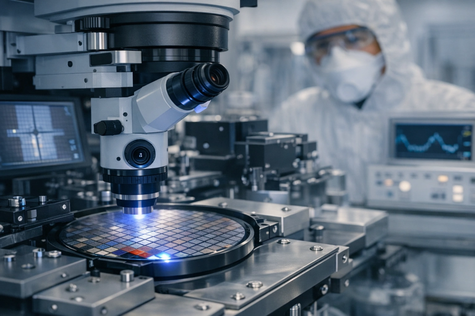
StructSure materials support advanced lithography, permanent coatings, and packaging workflows in modern fabs. Our photoresists, dielectric layers, and ancillaries maintain dimensional accuracy, adhesion, and stability under demanding cleanroom conditions.
Kayaku’s StructSure materials enable reliable wafer‑level and advanced packaging processes by delivering stable patterning, strong adhesion, and consistent film performance across critical backend steps. Our portfolio includes photo‑patternable dielectrics such as KMSF® 1000 and KMSF® 2000, along with plating resists and electrophoretic coatings designed for RDL formation, TSV metallization, and high‑density interconnect architectures. These chemistries are engineered to maintain dimensional accuracy and long‑term reliability, supporting the increasingly complex packaging workflows used in modern microelectronics manufacturing.
For III‑V and optoelectronic device fabrication, Kayaku provides a broad set of resists, dielectrics, and optical polymers optimized for high‑resolution patterning and structural precision. Materials such as PMGI/LOR lift‑off layers, SU‑8 epoxies, PMMA e‑beam resists, and Cyclotene® dielectrics support airbridges, T‑gates, waveguides, microlenses, and other compound semiconductor structures. Complementary optical materials—including OrmoClear® and hybrid polymers—extend capability into micro‑optics and photonic integration. These solutions are engineered to maintain profile stability and optical clarity, ensuring reliable performance across RF, photonics, and III‑V device workflows.
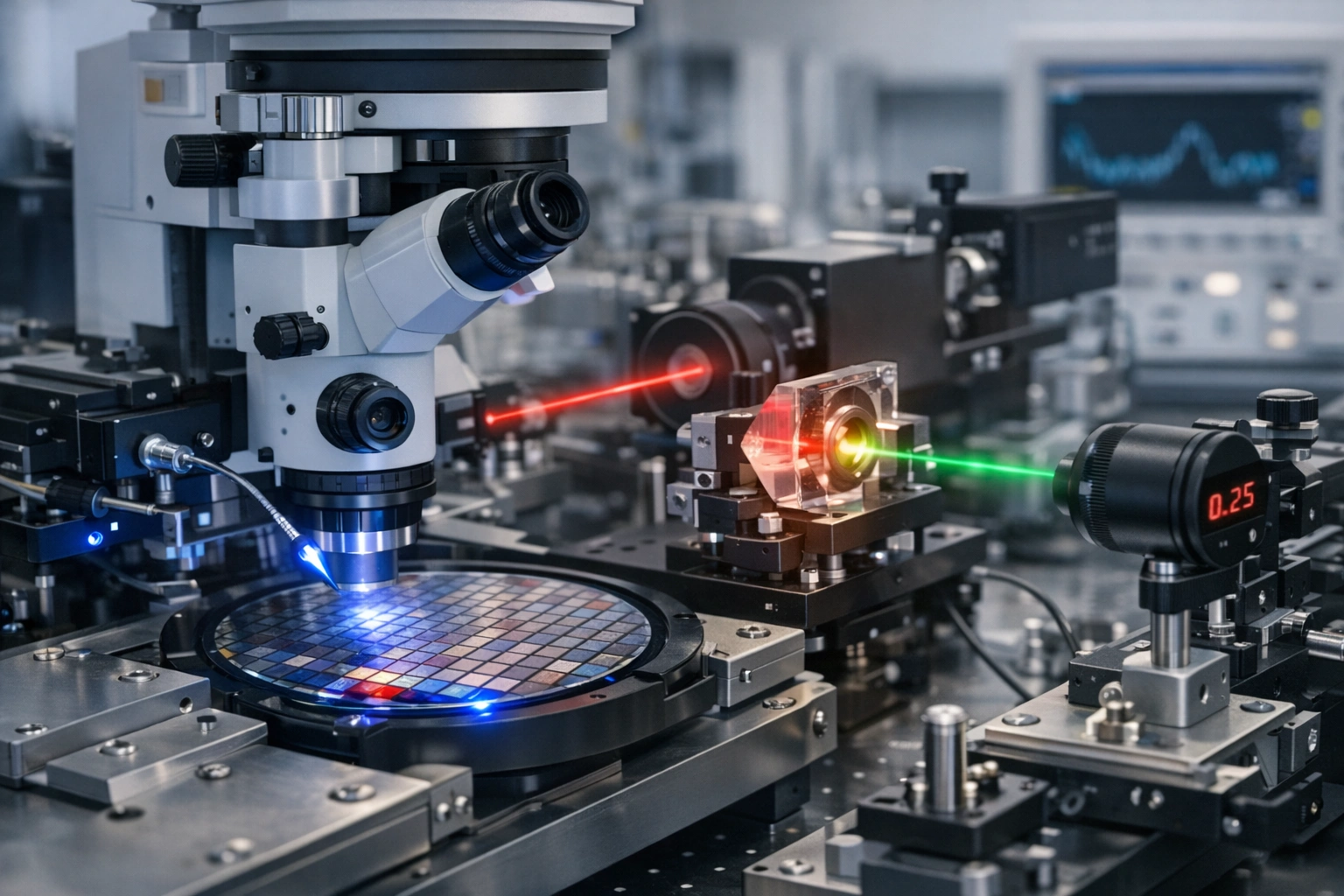
Lithography sits at the center of Kayaku’s materials expertise. The StructSure family spans SU‑8 and KMPR® permanent epoxies, lift‑off chemistries, PMMA for high‑resolution e‑beam, and a full suite of i‑line and DUV materials supplied through Qnity and MRT. These resists are designed for clean pattern transfer, stable sidewall profiles, and reliable adhesion under demanding cleanroom conditions. Whether used in MEMS, advanced microfabrication, direct‑write laser lithography, or high‑aspect‑ratio LIGA workflows, Kayaku’s materials deliver the dimensional control and process stability manufacturers require.