Why Dielectric Materials Remain One of Advanced Packaging’s Greatest Challenges
Advanced packaging dielectric materials have become one of the most significant engineering challenges in modern semiconductor packaging. As package architectures continue to increase in complexity, engineers require photo-patternable dielectric materials that simultaneously deliver excellent electrical performance, mechanical reliability, thermal stability, and manufacturability. Achieving this balance—not maximizing a single material property—has become one of the defining challenges in dielectric polymer development.
Meeting one of these requirements is relatively straightforward. Meeting all of them simultaneously is considerably more difficult.
This challenge is driving continued innovation in dielectric polymer development as advanced packaging technologies evolve toward higher densities, greater power levels, and increasingly complex architectures. Commercial dielectric platforms such as KMSF® 2000, along with ongoing polymer research, help illustrate how material innovation continues to address these evolving requirements.
Balancing Competing Material Requirements
The ideal dielectric would simultaneously provide:
- Low dielectric constant (Dk)
- Low dielectric loss (Df)
- High thermal stability
- Mechanical toughness
- Low residual stress
- Low moisture absorption
- High breakdown voltage
- Low-temperature processing
- Excellent lithographic performance
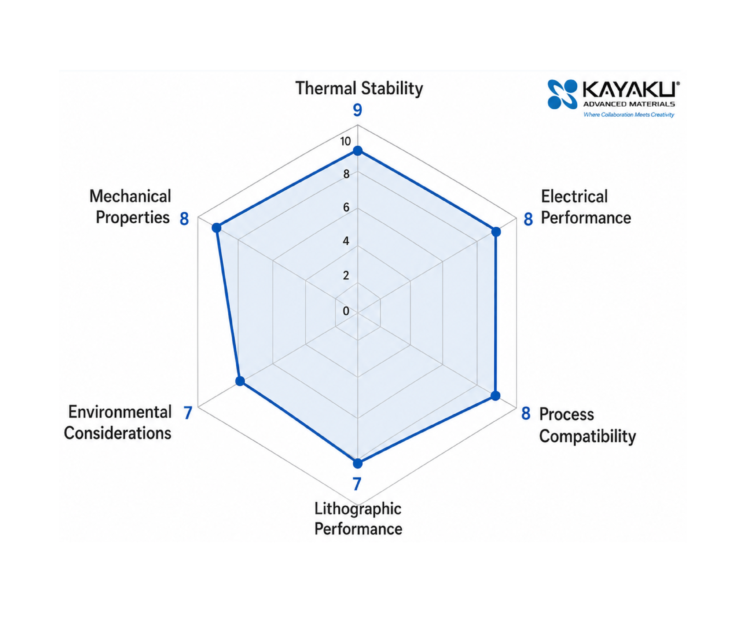
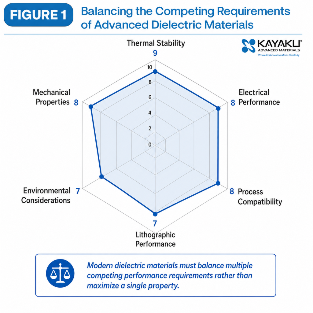
In practice, improving one property often comes at the expense of another. Increasing glass transition temperature (Tg) can increase film stress. Lower cure temperatures may reduce crosslink density. Materials optimized for lower dielectric constant can sacrifice mechanical strength, while tougher materials may exhibit higher dielectric loss.
Rather than maximizing a single performance metric, dielectric development has become an exercise in balancing multiple competing material requirements.
Figure 1 illustrates how modern dielectric development requires balancing multiple competing material requirements rather than optimizing a single performance metric.
Balancing the Next Generation of Dielectric Materials
At Kayaku Advanced Materials, our research focuses on developing dielectric polymers that balance these competing requirements while remaining compatible with existing semiconductor manufacturing processes.
Building on these material design principles, Kayaku Advanced Materials continues developing new dielectric polymer systems that balance electrical, mechanical, thermal, and processing performance while remaining compatible with semiconductor manufacturing.
KMSF® 2000: A Photo-Patternable Dielectric for Advanced Packaging
One example of this balanced design philosophy is the KMSF® 2000 dielectric platform. Originally developed for thin-film permanent dielectric applications, KMSF® 2000 demonstrated excellent lithographic performance across 3–10 μm film thicknesses while maintaining the balanced electrical, mechanical, and thermal properties required for advanced packaging.
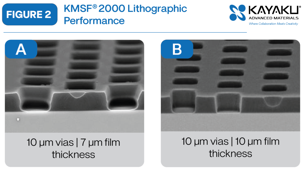
Building on this commercial platform, ongoing polymer research is exploring thicker dielectric structures while preserving the balanced electrical, mechanical, and thermal properties established by the original material.
Experimental polymer development has successfully demonstrated coating thicknesses up to 30 μm while achieving 2:1 aspect ratio patterning and maintaining the balanced material performance established by the original platform. These research results illustrate how continued polymer innovation can expand future design possibilities without fundamentally changing established processing approaches.
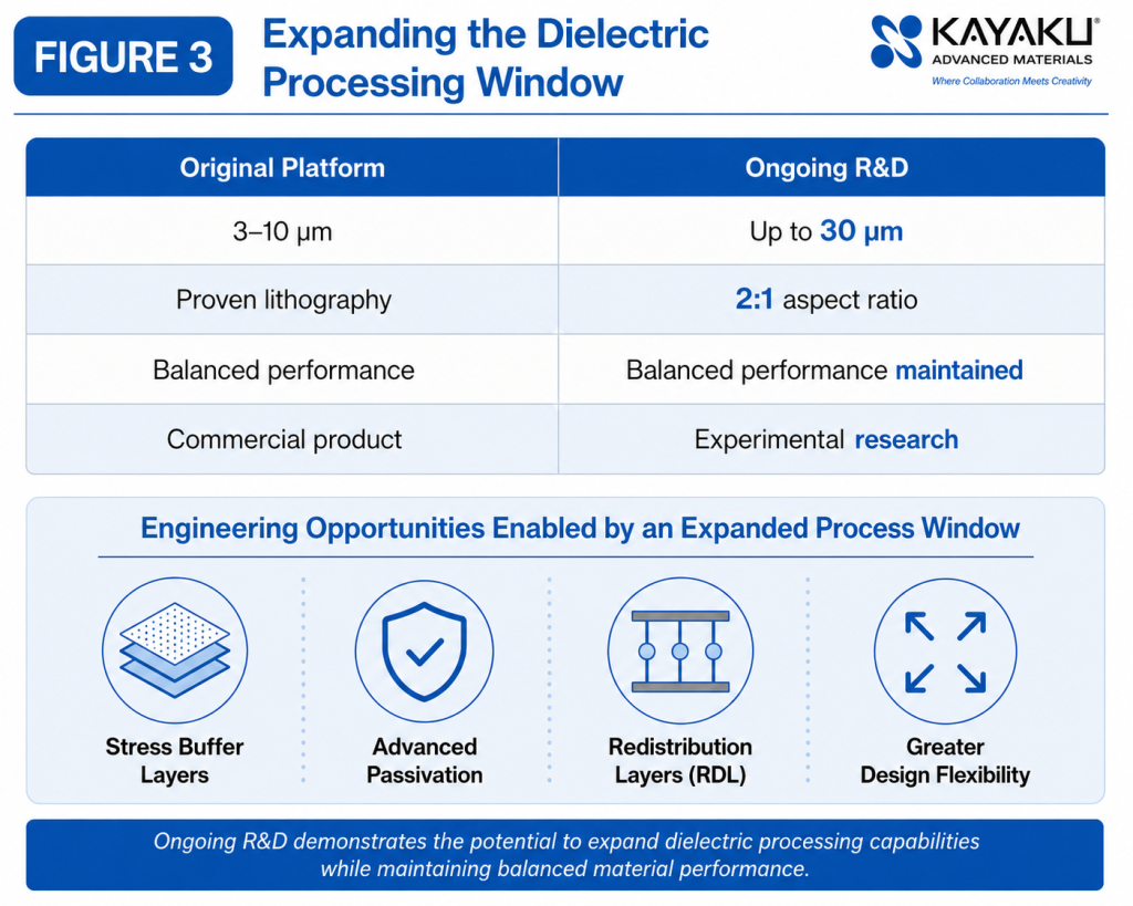
Instead of simply increasing thickness capability, an expanded processing window creates opportunities for thicker stress buffer layers, advanced passivation structures, redistribution layer (RDL) integration, and other packaging architectures where additional dielectric thickness can improve mechanical stress management and overall package reliability.
Looking Beyond Today’s Materials
While expanding processing capability is one avenue of development, polymer innovation extends well beyond a single material platform.
Kayaku Advanced Materials continues investigating a range of new polymer systems, including:
- Novel copolymer
- Pre-imidized polyimides
- Polybenzoxazoles
- Hybrid polymer architectures
Developing next-generation dielectric materials is no longer based solely on traditional trial-and-error experimentation. Today, computational modeling, large language models (LLMs), machine learning, and molecular modeling are integrated into the polymer development workflow to identify promising molecular structures, predict key material properties—including dielectric constant (Dk) and glass transition temperature (Tg)—and prioritize candidates before laboratory synthesis.
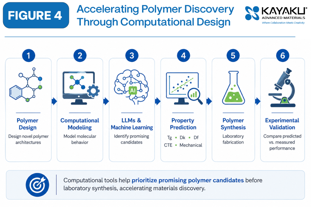
Rather than replacing traditional polymer chemistry, these computational tools complement experimental research by helping scientists focus laboratory efforts on the most promising polymer candidates. This integrated approach accelerates material discovery while improving confidence in predicting performance before synthesis.
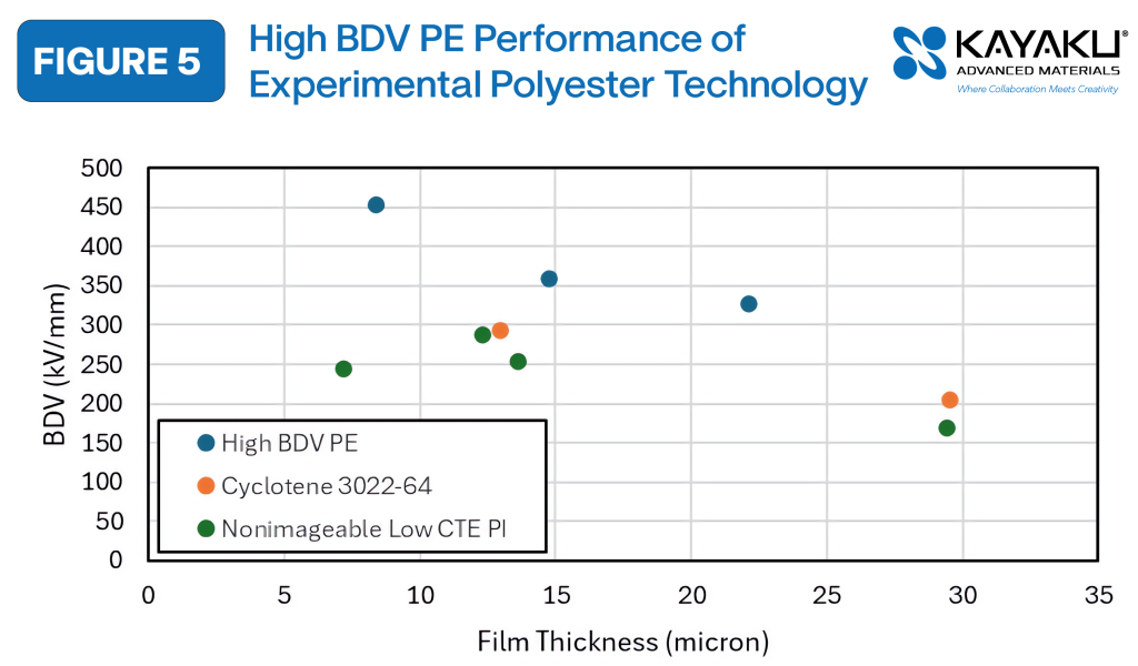
While many material properties must be optimized simultaneously, electrical reliability remains one of the most critical performance metrics for advanced dielectric materials. Breakdown voltage (BDV) represents the maximum electric field a dielectric can withstand before electrical failure occurs, making it particularly important for high-density and high-power semiconductor packaging applications.
One outcome of this research approach is the development of experimental high-breakdown-voltage copolymer systems. Early R&D results demonstrate promising electrical performance compared with commercially available dielectric materials, illustrating the potential of next-generation polymer architectures currently under investigation
Materials Designed for Tomorrow’s Packaging Challenges
Future semiconductor packaging will continue demanding materials that balance electrical performance, mechanical reliability, thermal stability, manufacturability, and environmental responsibility.
Research into expanded dielectric platforms—including the ongoing evolution of KMSF® 2000—demonstrates how advances in polymer chemistry can help address these competing requirements while remaining compatible with existing fabrication infrastructure.
The objective is not simply to maximize one property, but to engineer materials that deliver the right balance of performance across an increasingly complex set of design constraints.
Looking Ahead
Future dielectric development will increasingly depend on balancing electrical, mechanical, thermal, processing, and environmental requirements within a single material platform.
As advanced packaging technologies continue to evolve, the most successful dielectric materials will not be defined by a single outstanding property, but by their ability to deliver the optimal balance of electrical, mechanical, thermal, processing, and environmental performance.