KAM’s Design Fabrication Services (DFS) Group provides semiconductor fabrication services and characterization capabilities for engineers developing microelectronic, semiconductor, MEMS, and other advanced device technologies. By combining wafer processing, photolithography, thin-film processing, microreplication and molding—including small-substrate and hot embossing, soft lithographic molding, replica molding, and polymer microstructure replication—, inspection, reliability testing, and material characterization in one facility, DFS helps engineers evaluate materials and processes before moving toward larger-scale manufacturing.
Our Capabilities
KAM offers a broad range of in-house design, fabrication, processing, inspection, metrology, and material testing capabilities to support development from initial process evaluation through device fabrication and characterization.
Wafer Processing & Photolithography Machines and Tools
The Design Fabrication Services Group has a range of wafer processing and photolithography tools for developing and evaluating microfabricated structures across multiple wafer sizes. Our capabilities span surface preparation, coating and lamination, thermal processing, exposure, and development. All coming together to provide flexibility to support different materials, process conditions, and fabrication requirements.
Surface Preparation Machines & Tools
Surface preparation helps optimize substrate conditions before coating and patterning. DFS has in-house capabilities for both HMDS priming and plasma treatment across wafer-level substrates.
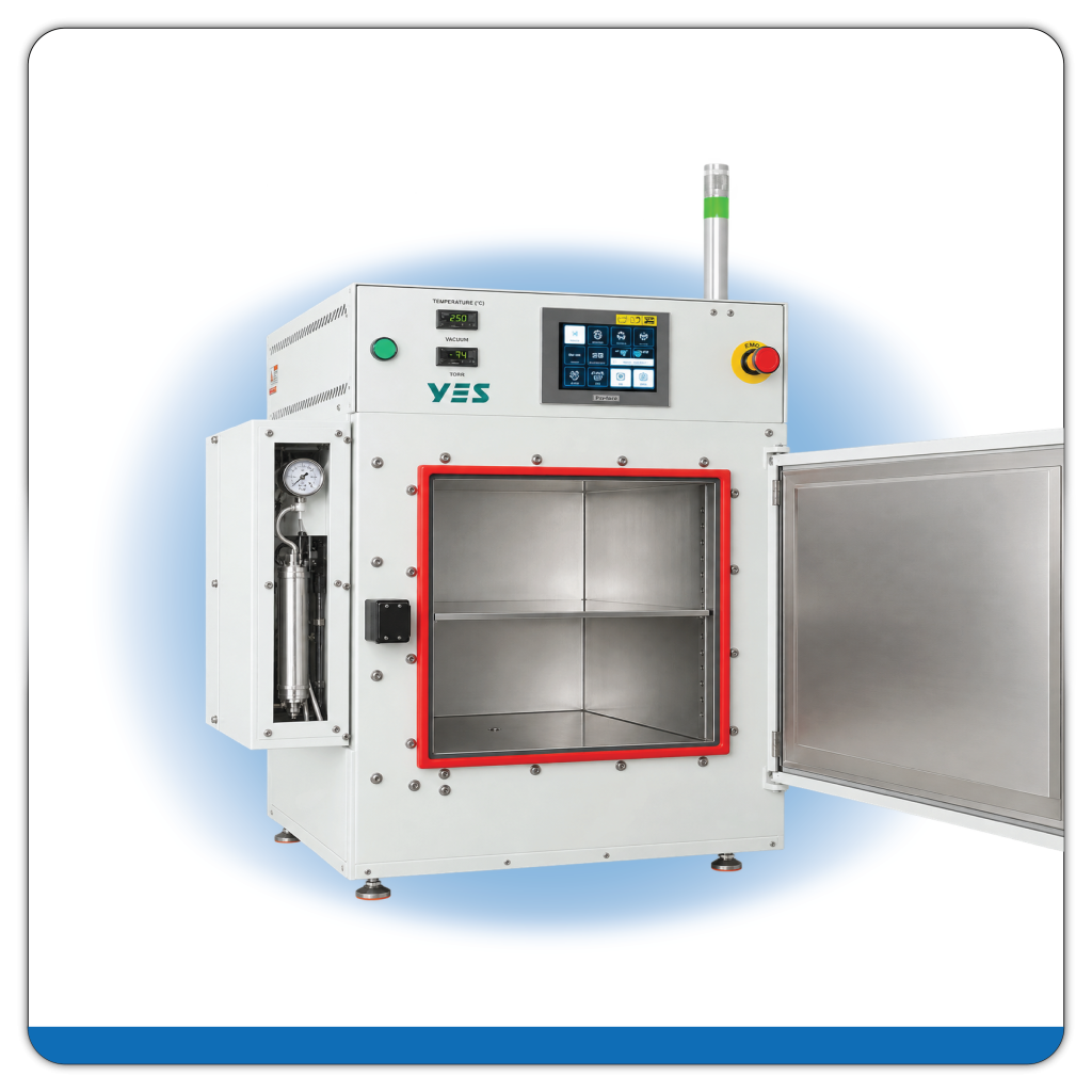
YES HMDS Oven
Up to 300 mm Wafers
Up to 310 x 310 mm Panels
Key Capability
HMDS Vapor Priming
Controlled HMDS vapor priming to improve surface conditions and promote adhesion of photoresist and other coatings for reliable subsequent processing.
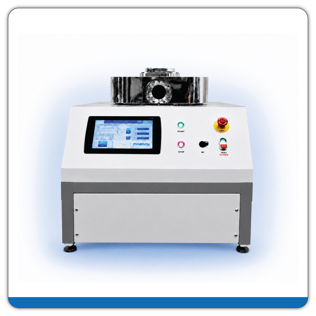
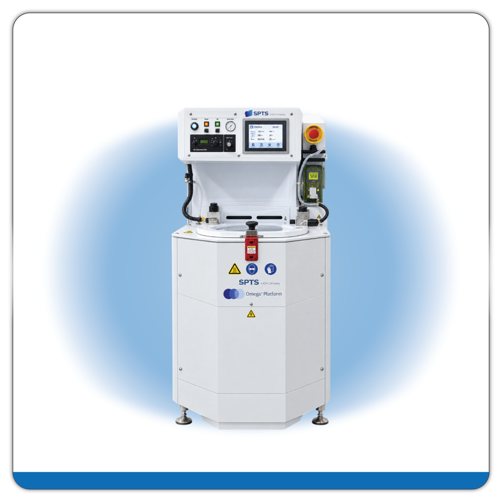
PVA PLASMA Tool
Up to 300 mm Wafers
Up to 310 x 310 mm Panels
Key Capability
Plasma Surface Treatment
Plasma treatment to clean and modify wafer surfaces, removing contaminants and enhancing surface properties to reliable subsequent processing.
Coating and Lamination Machines & Tools
DFS supports multiple methods for applying photoresists, dielectrics, and other functional materials to wafer-level substrates. Spin coating provides flexibility for liquid materials and controlled film formation, while lamination enables processing of dry-film and other film-based materials across a range of wafer sizes. These capabilities support photoresist processing, dielectric patterning, and other wafer fabrication applications.
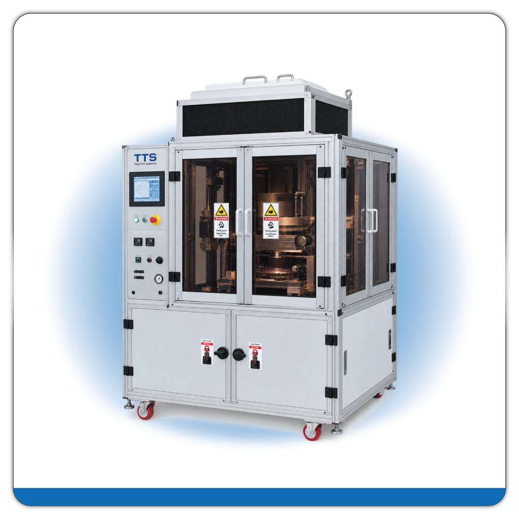
TTS Laminator
Up to 200 mm Wafers
Key Capability
Film Lamination
Wafer level lamination capability for applying film based materials to 4- or 8-inch wafers for subsequent fabrication and patterning processes.
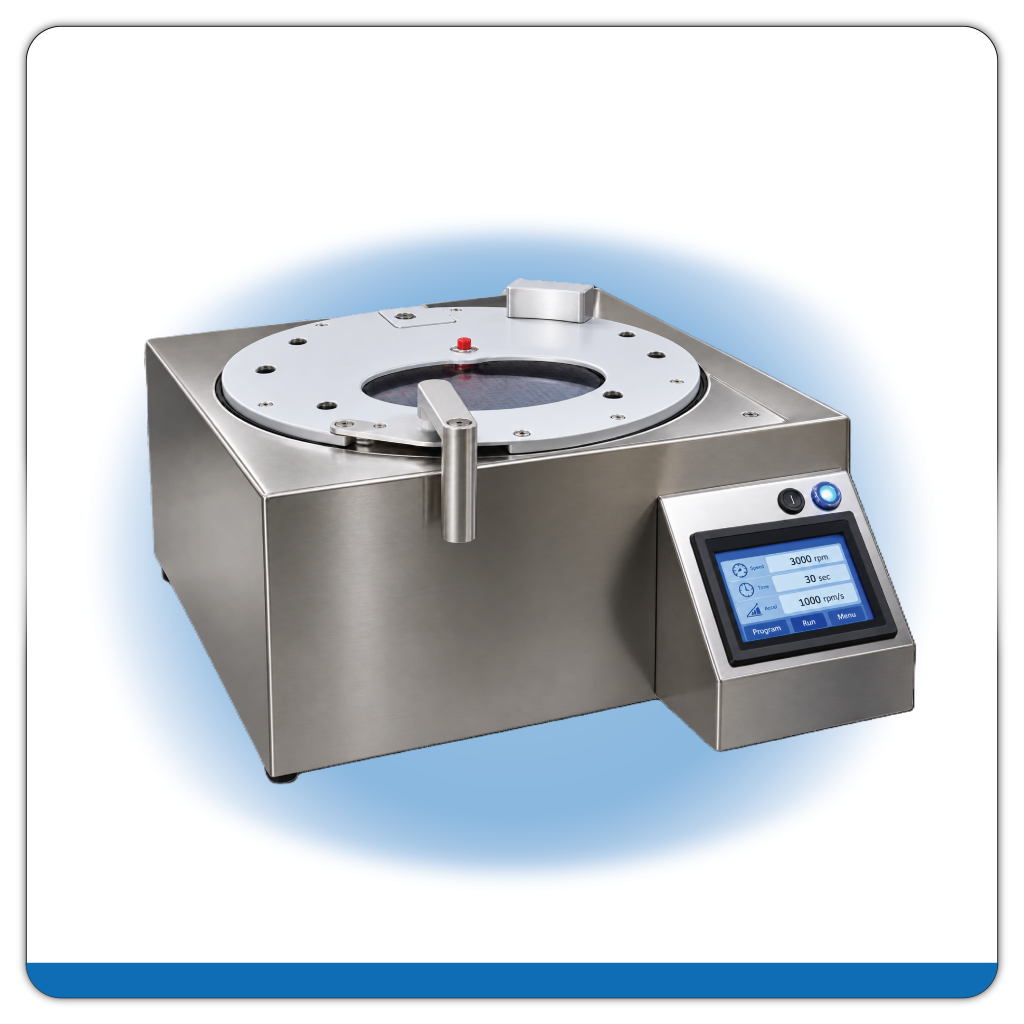
CEE 300X Spin Coater
Up to 12″ Wafers
Up to 310 x 310 mm Panels
Key Capability
Spin Coating
Spin coating capability for applying liquid photoresists, dielectrics, and other functional materials to wafer scale substrates.
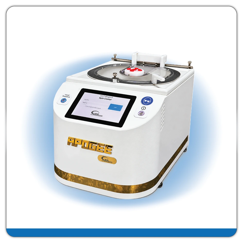
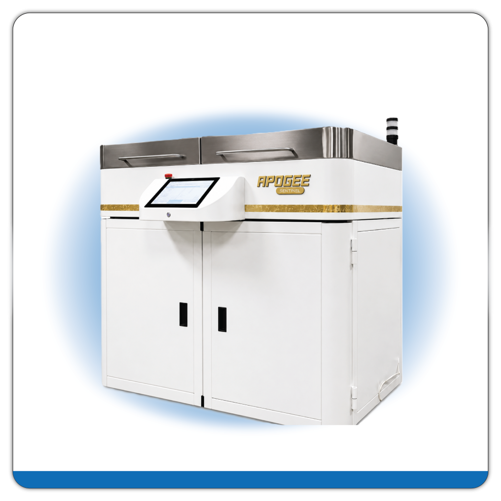
200X Apogee Spin Coater
Up to 200mm Wafers
Key Capability
Spin Coating
Spin coating for applying photoresists, dielectrics, and other functional materials to wafer-scale substrates.
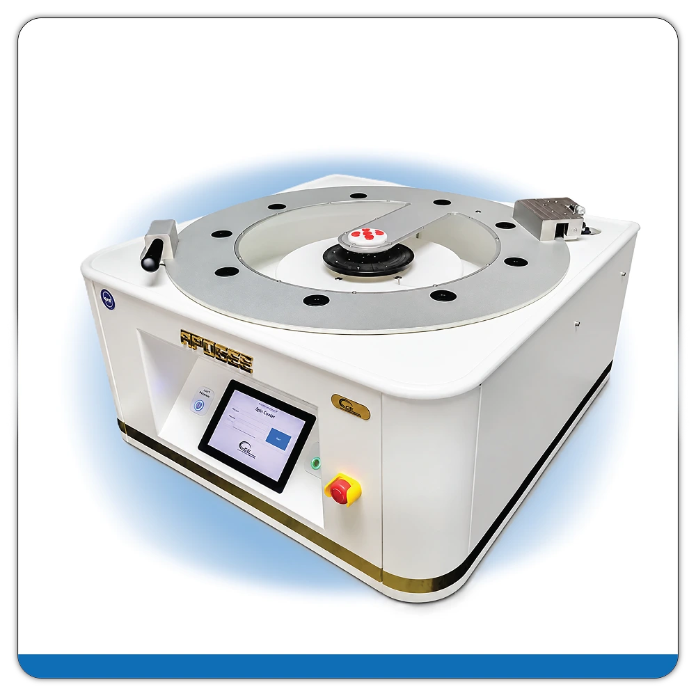
Apogee 450 Spin Coater
Up to 300 mm Wafers
Up to 310 x 310 mm Panels
Key Capability
Spin Coating
Spin coating for applying photoresists, dielectrics, and other functional materials to wafer-scale substrates.
Thermal Processing Machines & Tools
DFS maintains multiple thermal processing systems to support different stages of wafer and material processing. Capabilities include controlled baking, inert atmosphere processing, and vacuum processing for substrates up to 12 inches, providing flexibility for processes requiring different temperatures and environmental conditions.
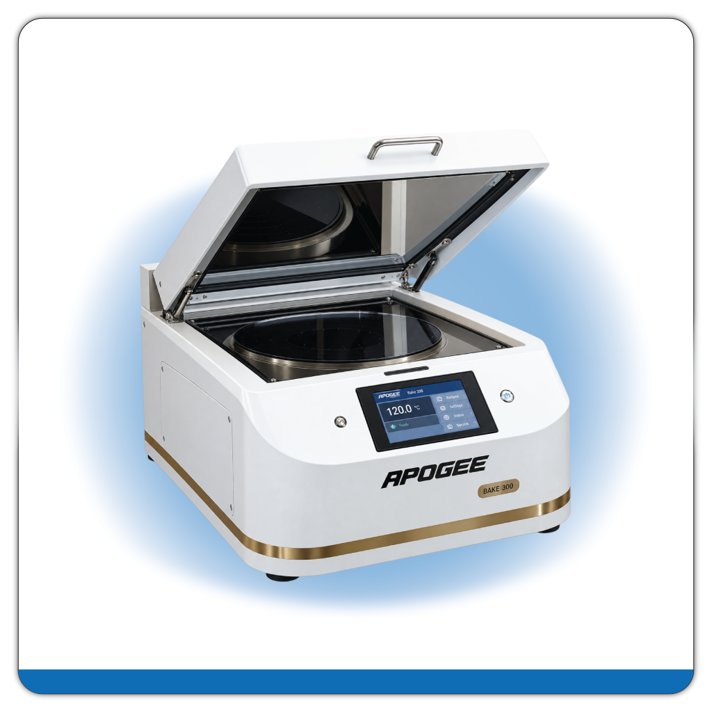
Apogee Bake 300
Up to 12″ Wafers
Up to 310 x 310 mm Panels
Key Capability
Controlled Wafer Baking
Controlled thermal processing for wafer-scale substrates, supporting bake steps used throughout photolithographic and microfabrication processes.
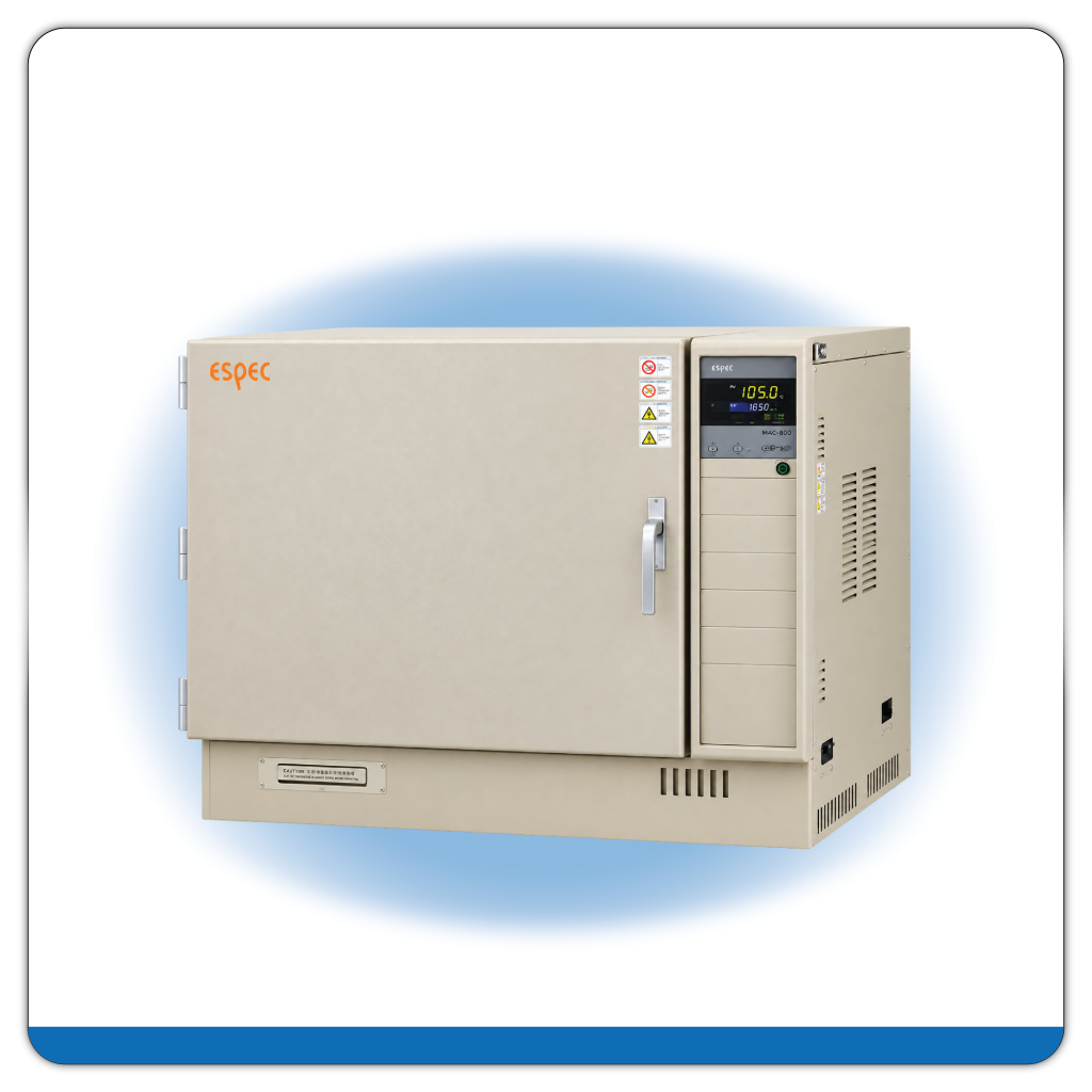
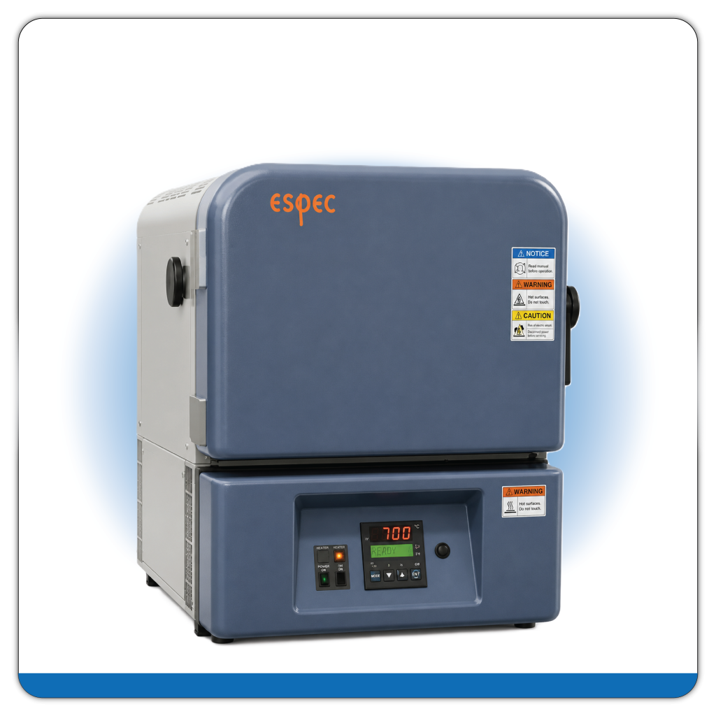
ESPEC Inert Oven
Up to 300 mm Wafers
Up to 310 x 310 mm Panels
Key Capability
Inert Atmosphere Processing
Controlled heating under an inert atmosphere for wafer and material processing where environmental control is important.
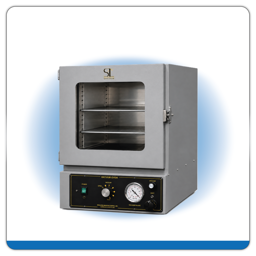
Sheldon Vacuum Oven
Up to 200 mm Wafers
Key Capability
Vacuum Thermal Processing
Vacuum-assisted thermal processing for wafer and material applications requiring controlled heating under reduced-pressure conditions.
Exposure Machines & Tools
Exposure is a critical step in photolithography, transferring patterns onto photoresist-coated substrates using controlled light sources and alignment systems. DFS maintains multiple exposure platforms to support different wafer sizes, exposure requirements, and process approaches, providing flexibility for developing and evaluating patterned structures.
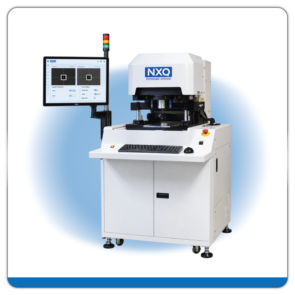
NXQ Exposure Tool
Up to 200 mm Wafers
Key Capability
Multi-Wavelength LED Exposure
LED-based exposure with selectable 356 nm and 405 nm wavelengths, including the ability to blend wavelengths. The system supports 4-, 6-, and 8-inch wafers for flexible photolithography processing.
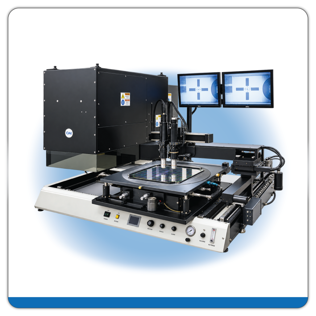
OAI Conatct Mask Aligner
Up to 300 mm Wafers
Up to 310 x 310 mm Panels
Key Capability
Contact Mask Alignment & Exposure
Contact mask alignment and exposure for transferring photolithographic patterns onto wafer-scale substrates. The system supports mask-based patterning for a range of microfabrication processes.
Development Machines & Tools
Following exposure, development removes the soluble portions of the photoresist to reveal the intended pattern. DFS has in-house development equipment capable of processing wafer-scale substrates, supporting a range of photolithographic materials and patterning requirements.
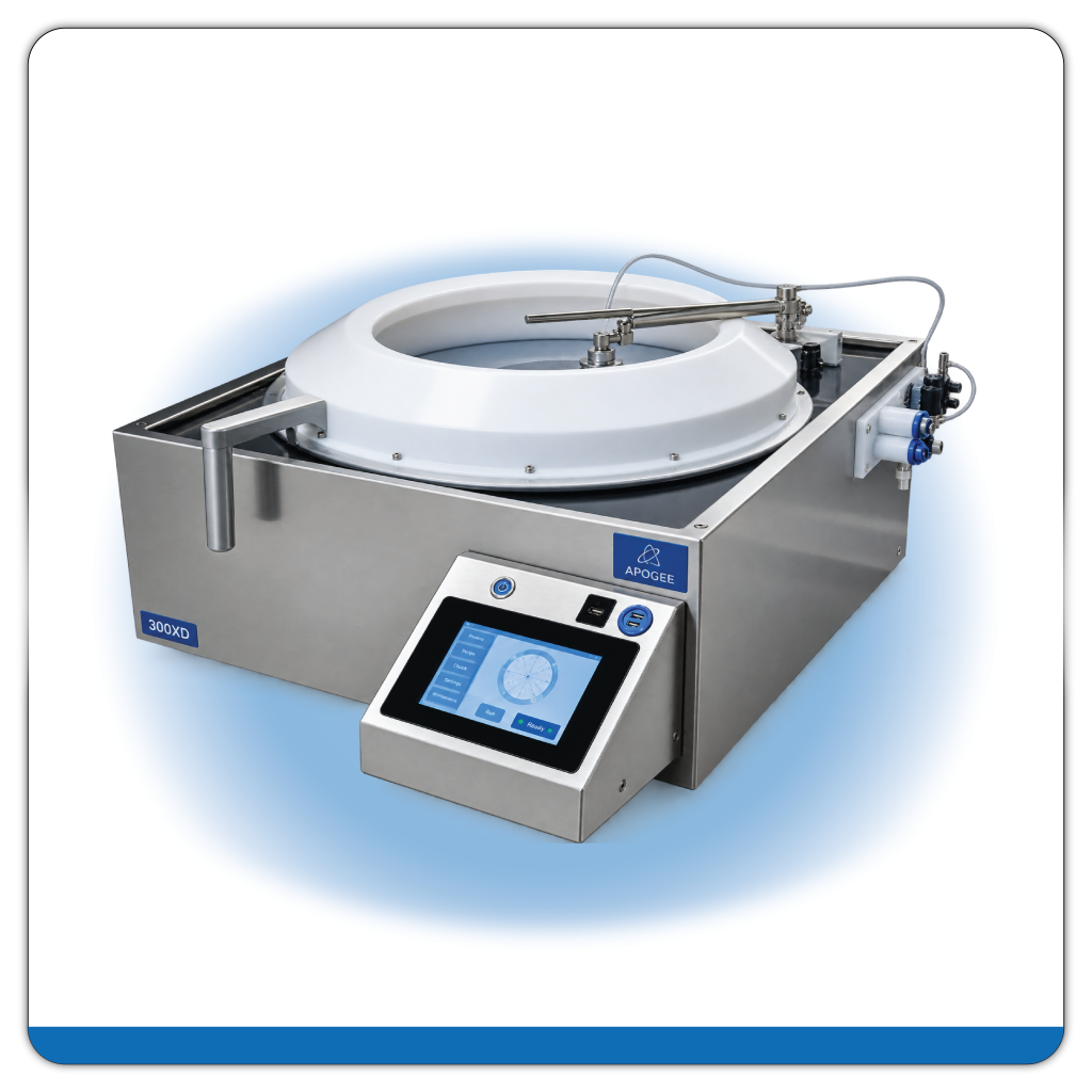
Apogee 300XD & 200X
Up to 300 mm Wafers
Up to 310 x 310 mm Panels
Key Capability
Automated Photoresist Development
Automated wafer development for removing exposed or unexposed photoresist, depending on the resist chemistry, to reveal patterned features following photolithographic exposure.
Inspection & Metrology Tools
Inspection and metrology capabilities enable engineers to evaluate patterned features, film thickness, surface characteristics, and dimensional performance throughout the fabrication process. These measurements help assess process results and identify variations that may affect device performance.
FilmTek Film Thickness Microscope
Up to 300 mm Wafers
Key Capability
Contact & Non-Contact Thickness Measurement
Measures thin-film thickness across wafer substrates using contact and non-contact measurement methods, supporting process control and characterization of deposited and coated materials.
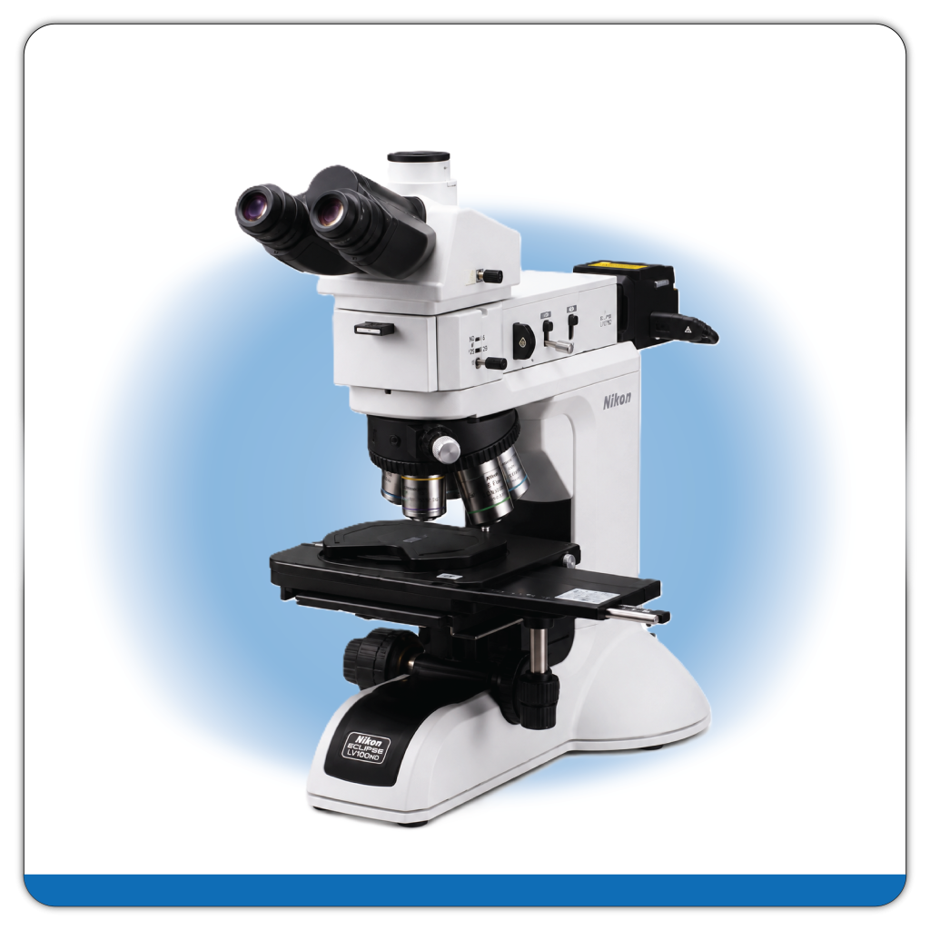
Nikon Optical Microscope
Up to 200 mm Wafers
Key Capability
High-Resolution Optical Inspection
Provides detailed optical inspection of wafers and fabricated structures for evaluating surface features, defects, pattern quality, and overall process results.
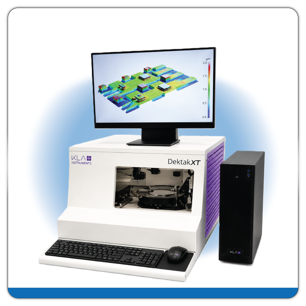
KLA-Tencor P-17 Surface Profilometer
Up to 200 mm Wafers
Key Capability
Step Height & Surface Profile Measurement
Measures surface topography and step heights to characterize patterned features, film thickness, and changes in wafer surface profiles.
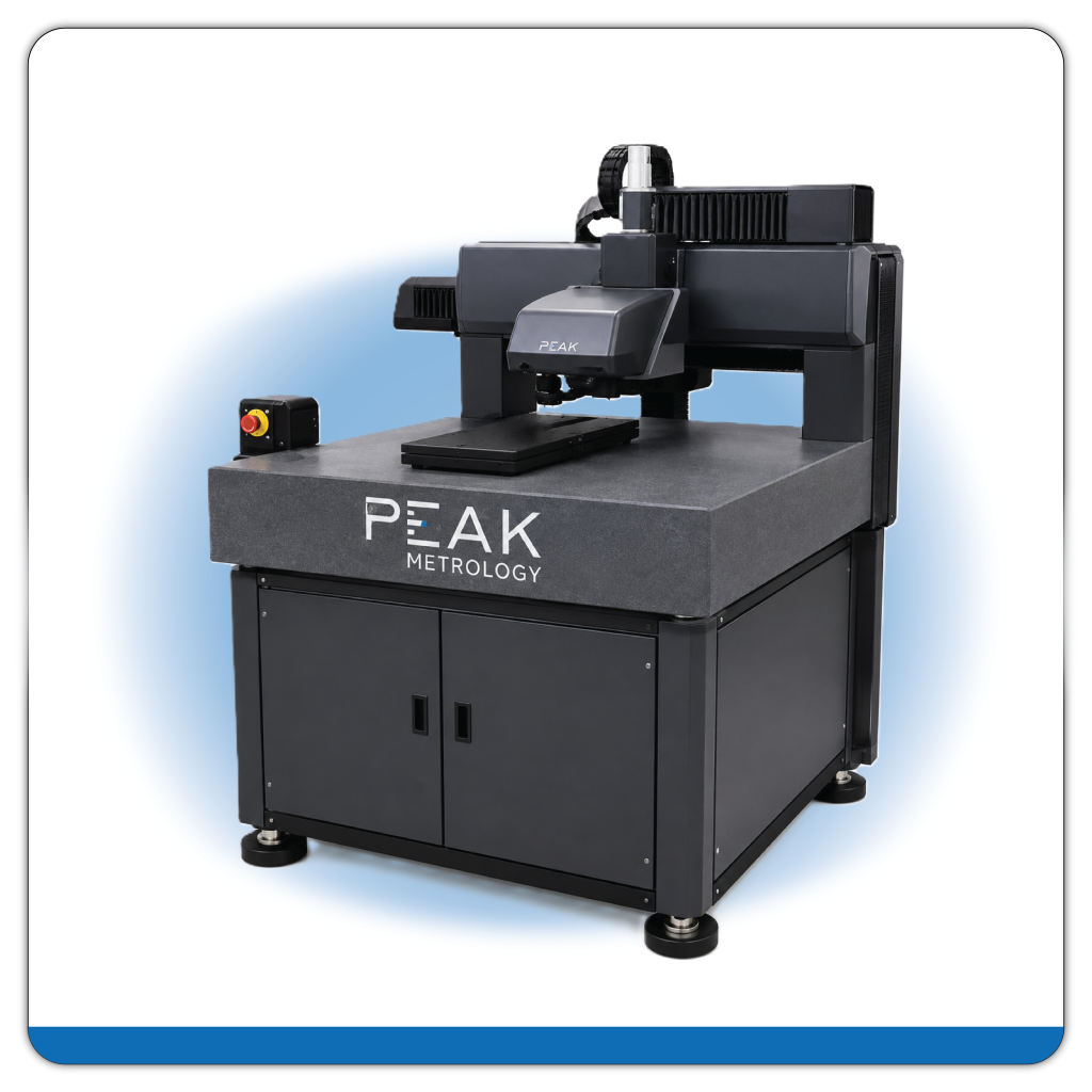
Keyence VK-X3000 3D Surface Profilometer
Up to 300 mm Wafers
Up to 310 x 310 mm Panels
Key Capability
3D Surface Profilometry
Provides three-dimensional surface measurements for evaluating feature geometry, surface roughness, height variation, and detailed topography of fabricated structures.
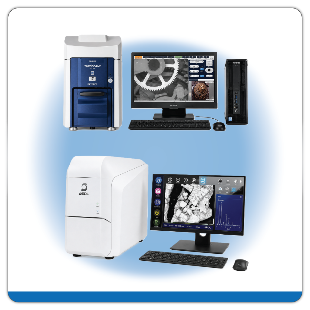
Hitachi TM4000 / JEOL JCM-7000
Key Capability
High Resolution Surface Imaging
Provides high-resolution imaging of microfabricated structures and surfaces for examining feature dimensions, pattern quality, defects, interfaces, and process results.
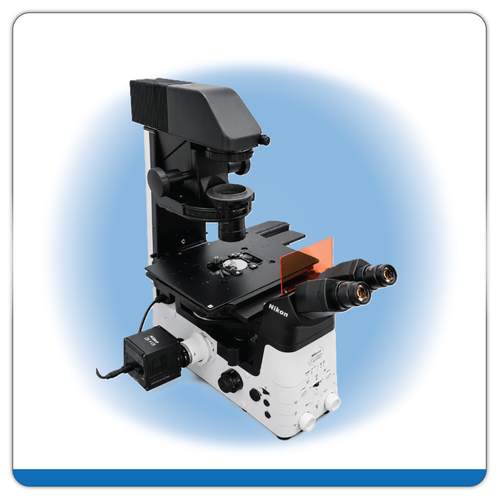
Nikon Ti2 Inverted Microscope
Up to 300 mm Wafers
Key Capability
Inverted Optical Microscopy
Optical inspection and characterization of wafers, surfaces, and microfabricated structures during process development and evaluation.
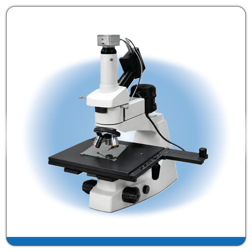
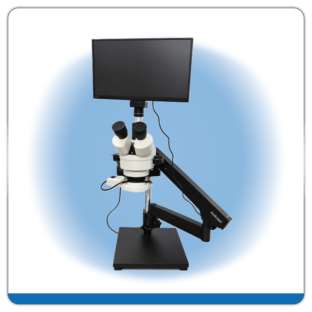
Bonding Microscope
Up to 300 mm Wafers
Key Capability
Wafer Bonding Alignment & Inspection
Microscopic alignment and inspection of wafers and bonded interfaces to support wafer bonding processes and device fabrication.
Reliability Tools
KAM’s reliability capabilities evaluate materials, processes, and devices under accelerated environmental, thermal, and humidity conditions to identify potential reliability risks and failure mechanisms.
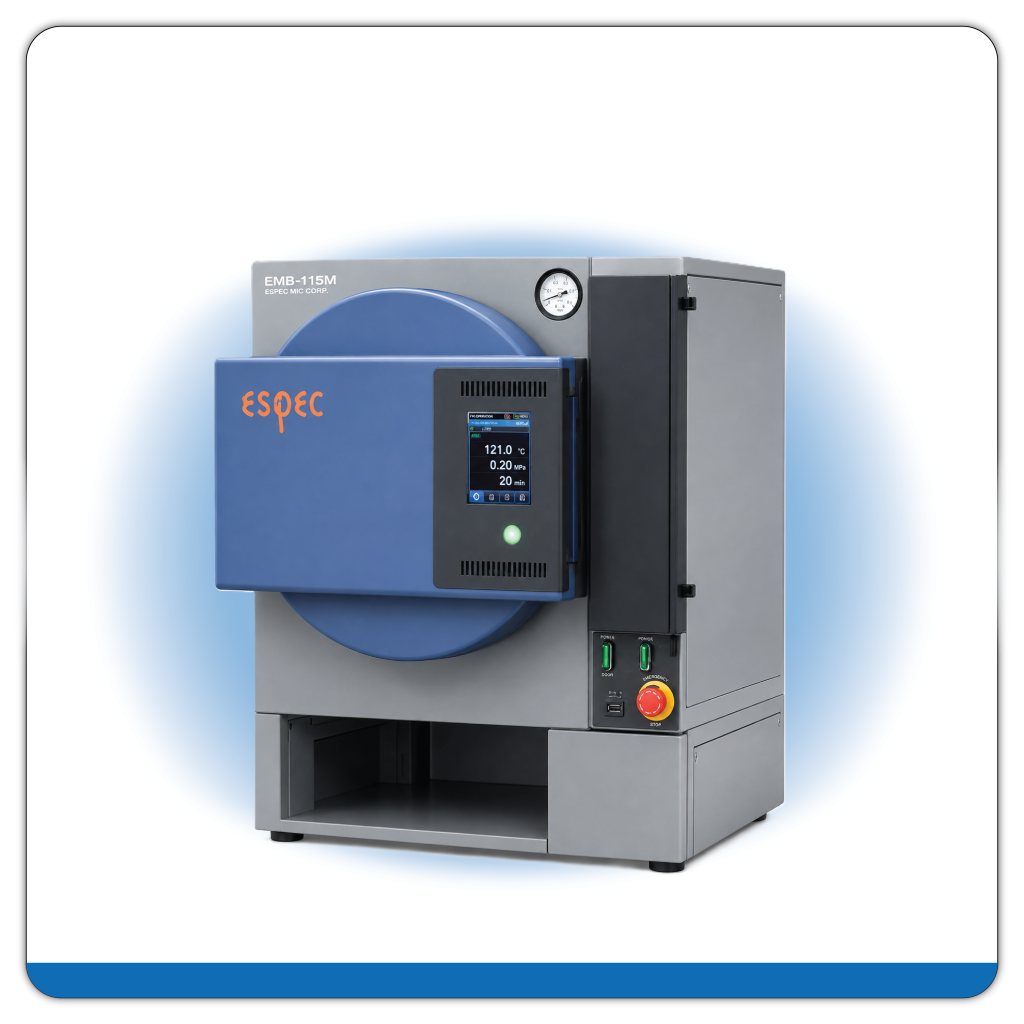
ESPEC HAST Chamber
Up to 300 mm Wafers
Up to 310 x 310 mm Panels
Key Capability
Highly Accelerated Stress Testing
Accelerated environmental testing under elevated temperature and humidity conditions to evaluate material and device reliability and identify potential failure mechanisms.
ESPEC Thermal Cycle Chamber
Up to 300 mm Wafers
Up to 310 x 310 mm Panels
Key Capability
Thermal Cycling
Controlled temperature cycling to evaluate materials and devices under repeated thermal expansion and contraction conditions.
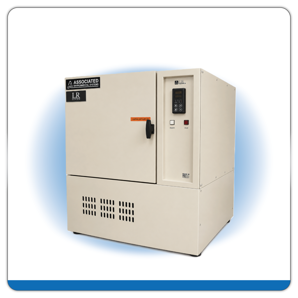
LR Environmental Chamber
Up to 300 mm Wafers
Up to 310 x 310 mm Panels
Key Capability
Environmental Reliability Testing
Controlled environmental testing for evaluating material and device performance under temperature and humidity conditions representative of demanding operating environments.
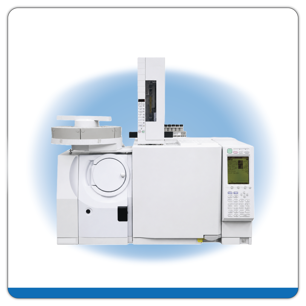
GCMS Gas Chromatography Mass Spectrometry System
Key Capability
Chemical Analysis & Material Charcaterization
Controlled environmental testing for evaluating material and device performance under temperature and humidity conditions representative of demanding operating environments.
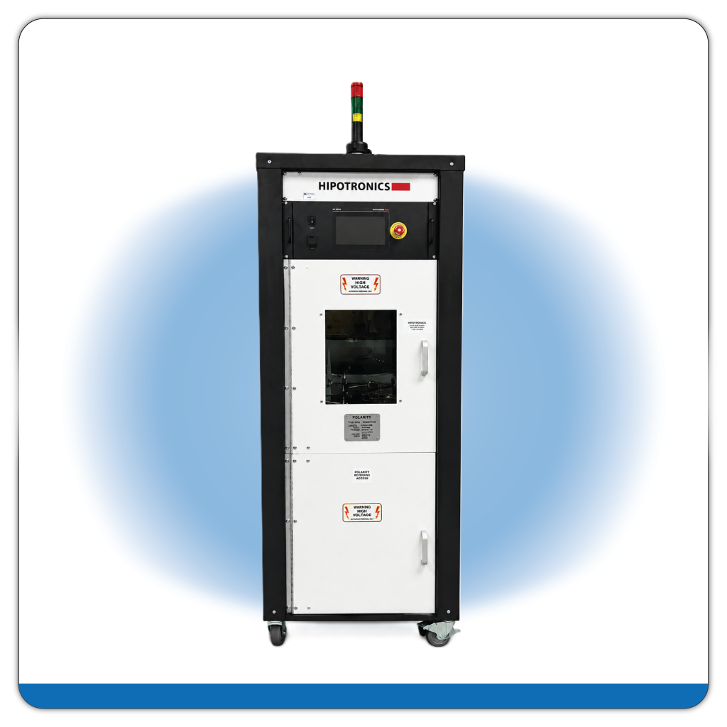
HIPTRONICS Breakdown Voltage Tool
Key Capability
Environmental Reliability Testing
Controlled environmental testing for evaluating material and device performance under temperature and humidity conditions representative of demanding operating environments.
Other Applications & Processing Tools
KAM’s additional processing capabilities support specialized fabrication requirements, including thin-film deposition, plating, wafer bonding, and de-bonding. These tools provide additional process steps for developing and evaluating advanced materials and device fabrication approaches.
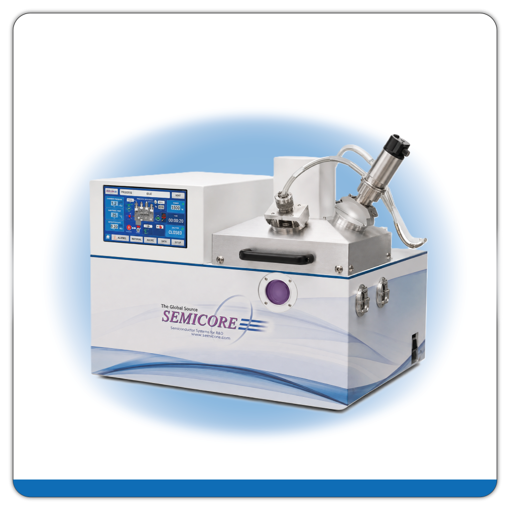
Semicore Sputter Tool
Up to 200 mm Wafers
Key Capability
Thin-Film Deposition
Physical vapor deposition (PVD) for depositing thin metal and other functional films onto substrates. Supports material deposition for metallization, electrodes, and other device fabrication applications.
Technic Plating Tool
Up to 200 mm Wafers
Key Capability
Electroplating & Metal Deposition
Electrochemical plating for depositing metal films onto patterned substrates. Supports applications requiring controlled metal buildup for semiconductor and microfabrication processes.
Apogee Bonder & De-Bonder
Up to 200 mm Wafers
Key Capability
Wafer Bonding & De-Bonding
Wafer bonding and de-bonding capabilities for temporary or permanent substrate integration. Supports advanced packaging, wafer-level processing, and device fabrication workflows.
Material Testing Capabilities
KAM provides in-house material testing and characterization for evaluating physical, electrical, mechanical, thermal, analytical, and reliability properties. These testing capabilities help engineers characterize materials, compare formulations, evaluate process performance, and identify potential material-related issues during product and process development.
Physical &
Mechanical
Testing
Capabilities
Coating stress
Adhesion / shear testing
Chemical resistance
Electrical
Testing
Capabilities
Dielectric testing (Dk and Df up to 50 GHz)
Breakdown voltage
Conductivity
Thermal &
Mechanical
Testing
Capabilities
TGA
TMA
DMA
DSC
Tensile testing
Analytical Testing Capabilities
Analytical testing provides detailed characterization of material composition and physical properties to support formulation, processing, and performance evaluation.
Spectroscopy
Capabilities
UV-VIS spectroscopy
FTIR spectroscopy
Chromatography
Capabilities
GPC
GC
HPLC
Physical &
Chemical Testing
Capabilities
Refractometry
Surface tension
Particle counting
Particle sizing
Percent solids
Viscosity (kinematic and dynamic)
Density testing
Supporting Development from Process Evaluation to Fabrication
Developing advanced materials and microfabricated devices often requires evaluating multiple process steps and material properties together. KAM’s in-house fabrication, processing, inspection, metrology, reliability, and material testing capabilities allow engineers to evaluate these variables within a connected development environment. This integrated approach can help accelerate process development, troubleshoot fabrication challenges, and evaluate materials under application-relevant conditions.