Overview
Selecting a single-layer or bi-layer lift-off process begins with two practical questions: can the resist maintain a break in the deposited film, and can it do so at the required feature dimensions and pitch? The deposition equipment and recipe determine how much sidewall protection is needed. The line and space dimensions determine how much undercut the remaining resist can tolerate. A profile that works with directional evaporation may fail under sputtering, while an undercut large enough for the deposition may be impractical for a dense pattern.
Single-layer processing can reduce cost, steps, and cycle time. A bi-layer stack adds another way to control the undercut and support more demanding deposition conditions. Neither is universally better, and sputtering does not automatically require a bi-layer process. The correct choice depends on actual deposition geometry, film stack, resist support, minimum line/space, pattern pitch, and required feature quality.
Why the Deposition Tool Matters
Lift-off depends on a break between the film deposited on the substrate and the film deposited on top of the resist. That break is easier to preserve when arriving material is directional and harder when material reaches the resist sidewalls from a broad range of angles.
| Deposition method | Typical deposition behavior | Implication for lift-off |
|---|---|---|
| Thermal or e-beam evaporation | Generally line-of-sight, with relatively limited sidewall coverage. Source geometry, wafer tilt, and rotation still matter. | Often compatible with single-layer lift-off if the resist profile, deposited thickness, and feature geometry provide sufficient separation. Bi-layer can still help with thicker or more demanding stacks. |
| Sputtering | Usually broader angular distribution and more sidewall coating; results depend on pressure, target distance, collimation, substrate orientation/motion, and recipe. | A controlled undercut is more important, but its width must fit the line/space geometry. A single-layer profile may be sufficient where the necessary undercut is compatible with minimum feature dimensions and pitch; use bi-layer when additional undercut control is required. |
| Highly conformal methods (e.g., ALD or many CVD processes) | Material covers the resist top, walls, and potentially the underside of overhangs. | Neither single-layer nor bi-layer lift-off can be assumed to work. Revisit deposition conditions or evaluate a deposition-then-etch patterning route. |
The important consideration is the sidewall coverage produced under the actual deposition conditions. Sputtering may provide adequate directional control in certain configurations, while evaporation can still produce bridging depending on deposition geometry.
Profile control in single-layer and bi-layer processing
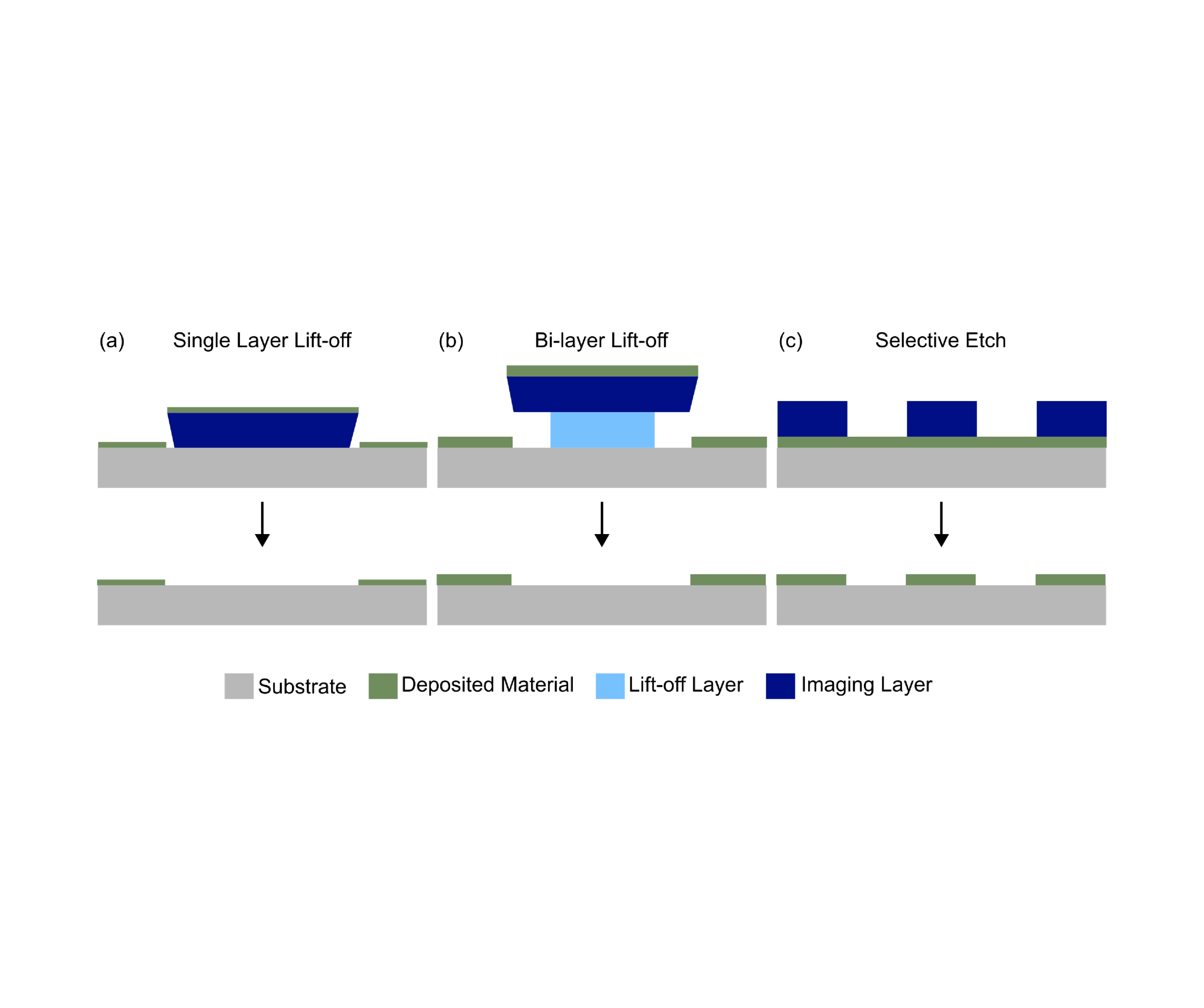
In single-layer lift-off, one imaging resist supplies the mask and the needed sidewall shape. A suitably designed negative-tone or image-reversal resist can produce a re-entrant or undercut profile without a separate lift-off layer. Thus, single-layer processing can incorporate an undercut profile.
In a bi-layer process, a separately dissolving underlayer—commonly PMGI/LOR—sits beneath an imaging resist. Controlled lateral dissolution of the underlayer creates an overhang. This allows profile tuning beyond what the imaging layer alone may provide, but it adds coating, baking, development, interlayer compatibility, and removal variables.

Undercut requirements and feature geometry
The achievable undercut is constrained by feature dimensions and pitch. Increasing the undercut improves separation between the deposited film on the substrate and resist, but reduces the supporting width beneath the remaining resist features. At smaller feature widths and pitches, excessive undercut can compromise pattern stability and dimensional control. This limitation applies to both single-layer and bi-layer processes.
For a simplified symmetric profile, a resist bridge of nominal top width W with an undercut u on each side has a remaining base width of approximately W – 2u. This is a geometric illustration, not a universal design rule: the usable limit also depends on height, profile shape, mechanical stiffness, adhesion, deposition stress, and process variation. Pitch by itself is insufficient; line width, space width, and pattern duty cycle determine which resist bridges must survive.
Single-layer UniLOR® N can produce a substantial undercut and support lift-off for certain sputtered films. However, an undercut appropriate for a given deposition process may not be compatible with the minimum resist feature width or pitch. A bi-layer enables more independent adjustment of undercut relative to the imaging profile, but excessive lateral dissolution can still compromise support beneath narrow features. KAM’s high-temperature sputtering work notes that large undercut ratios may lead to loss of smaller features [3].
Beyond deposition method: five additional selection factors
- Film thickness and stack construction. Thicker metal or oxide stacks increase the risk that deposits on the resist top, sidewall, and substrate connect. The available resist height and undercut must be evaluated against the total deposited stack, not just one layer.
- Thermal and mechanical loading. Substrate temperature, energetic particle bombardment, deposition duration, and film stress can soften, distort, or collapse the resist profile. Robustness is formulation- and process-specific; a second layer does not automatically solve it.
- Pitch, resist-bridge width, and substrate topography. Undercut acts laterally into the resist feature from both sides, so a narrow remaining resist bridge can lose its supporting base. Dense line/space patterns may therefore rule out the undercut needed for a given deposition recipe. Stepped surfaces also modify deposition coverage.
- Materials and removal compatibility. Metals, oxides, adhesion layers, and deposited multilayers behave differently. Confirm that the resist withstands the deposition and that removal solvents and agitation will not damage the deposited film or substrate.
- Required pattern quality and production margin. A process must meet edge definition, critical dimension (CD), particle/residue, defect, and wafer-level yield specifications—including at the minimum required feature dimensions.
Practical selection guide
| Starting Conditions | Reasonable first choice | What must be verified |
|---|---|---|
| Directional evaporation, relatively thin film, modest thermal load | Single-layer resist with a qualified re-entrant or suitable steep profile. | Clean film separation, CD, edge quality, and repeatability across the wafer. |
| Sputtering; moderate thickness; relatively generous line/space | Single-layer undercut may work if the width and stability of remaining resist features are adequate. | Verify sidewall break, undercut width, narrowest resist bridges, CD, lift-off residue, and yield. |
| Dense or fine-pitch features needing substantial undercut | Optimize deposition directionality and profile first; choose a structure that preserves both separation and resist support. | Check whether the required lateral undercut is feasible inside minimum feature spacing; test the smallest pitch and worst-case pattern density. |
| Thick, multilayer, or high-temperature / high-stress sputtering | Consider a robust bi-layer design early, with profile, thermal resistance, and undercut sized for the stack. | Undercut survives the deposition, top resist remains supported, and lift-off meets yield and edge requirements. |
| Strongly conformal deposition / persistent sidewall encapsulation | Do not default to ever-larger undercut. Reconsider deposition settings or use etch-based patterning. | Demonstrated physical discontinuity and remover access, or a qualified alternative process. |
These recommendations depend on the deposition conditions, film stack, and minimum pattern geometry. Single-layer processing is appropriate when it satisfies the required lift-off specifications with adequate margin; a bi-layer is appropriate when additional profile control is necessary to meet those specifications.
Example from KAM application work
KAM has demonstrated that a single-layer UniLOR® N 5.0 process can generate substantial undercut through adjustments to exposure and development conditions [1]. Such profiles may support less-directional deposition, including certain sputtering processes. The feasible undercut is nevertheless limited by the minimum resist feature dimensions and pitch, because lateral dissolution reduces the support available beneath narrow resist features.
For demanding sputtered oxide stacks, KAM has also documented a bi-layer combination of LOR 30C and UniLOR® N 5.0, including a 3.75 μm Ta₂O₅/SiO₂ deposition at approximately 180°C using a 6 μm LOR layer and 8 μm UniLOR layer [2]. In this case, the added layer provides profile control needed to maintain undercut through substantial film thickness, temperature, and deposition stress. Additional KAM work addresses high-temperature sputtered optical coatings [3].
Qualification sequence
- Specify the deposition tool and recipe. Record sputtering versus evaporation; source geometry; pressure; substrate tilt and rotation; collimation; temperature; and deposition duration.
- Define the film and pattern requirements. List deposited materials and total thickness; thermal and stress limits; minimum deposited line/space and pitch; the corresponding narrowest resist bridge; topography; and acceptable edge/particle defects.
- Select and measure the resist profile. For both candidates compare the undercut needed to break sidewall coverage against the maximum undercut that preserves the narrowest resist feature. Measure resist thickness, cross-section, undercut, base width, and CD before deposition.
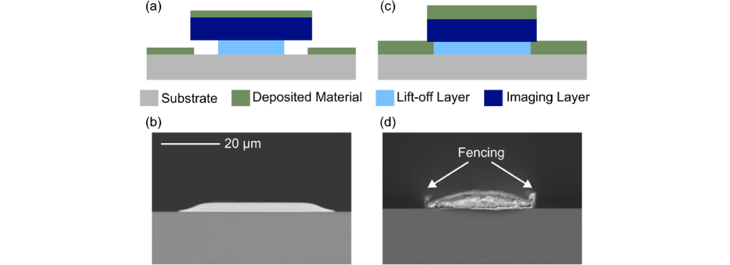
- Deposit, lift off, and measure the result. Check bridging and resist distortion after deposition, then assess fencing, edge roughness, lift-off residue, CD shift, and across-wafer yield after removal.
- Choose the simplest qualified process. Keep single-layer if it meets the requirements with process margin. Use bi-layer when it resolves an observed failure mode. If neither works, change deposition conditions or patterning approach.
Selection principle. Deposition conditions and the deposited film stack determine the undercut required to avoid sidewall bridging, while feature dimensions and pitch limit the undercut that can be accommodated. Single-layer processing may be suitable for sputtering when it achieves the required discontinuity without compromising resist support. Bi-layer processing permits greater flexibility in undercut control but remains subject to the same dimensional constraints. Select the architecture that demonstrates reproducible, clean lift-off at the minimum required feature dimensions.
Downloads
References
[1] Large Undercut Lift-off Processing using UniLOR N 5.0. Kayaku Advanced Materials, (2026). https://kayakuam.com/application-notes/large-undercut-lift-off-processing-using-unilor-n
[2] Thick Film Depositions Via Bi-layer Lift-off Resist Processes, Kayaku Advanced Materials, (2026). https://kayakuam.com/application-notes/thick-film-deposition
[3] UniLOR® N Thermal Stability for Single Layer and Bi-layer Lift-off Processes, Kayaku Advanced Materials,(2026). https://kayakuam.com/application-notes/unilor-n-thermal-stability-lift-off
[4] A. Rendos et al. Proc. of SPIE , 13899, (2026). doi: 10.1117/12.3079850