

Photoresists & Specialty Chemicals
Thick Film Depositions Via Bi-layer Lift-off Resist Processes
Part of the Applications Notes LineBi-layer Metal & Oxide Depositions
The bi-layer lift-off method has been used successfully to commercially fabricate many structures including source, drain ohmic contacts, gates and air bridges for use in GaAs, GaN, InP, MEMS and other semiconductor devices. It is widely adopted for common pattern metallization processes. The process utilizes PMGI/LOR plus an imaging resist to create a dual layer masking structure.
Thick metal and oxide depositions have become increasingly relevant in the fabrication of next generation VCELS, sensors and optical layers. The bi-layer combination, of LOR 30C as the underlayer and UniLOR® N5.0 as the top imaging resist, is especially suited for metal or oxide depositions ≥ 5 µm using sputter or evaporation. For this type of process, it is necessary to have a thick and robust resist stack to withstand the higher stresses of thick and/or high temperature depositions.
LOR 30C: Benefits/Attributes
- Thick PMGI-based sacrificial layer with high temperature stability
- Suitable for coating into trenches or over topography
- Excellent adhesion to a variety of substrates
- Suitable for bi-layer processes with top imaging resist (no intermixing)
- Clean removal
UniLOR® N5.0: Benefits/Attributes
- Thick negative-tone imaging resist
- Suitable as top imaging resist in bi-layer stacks
- Tunable profile
- Capable of maintaining pattern stability at higher temperatures
Thick Bi-layer Lift-off Process with LOR 30C/UniLOR® N5.0
LOR 30C and UniLOR® N5.0 create a highly robust bi-layer stack that is capable of withstanding high temperature (up to ~180˚C), high stress deposition processes and offers a controllable profile through key process parameters (See Fig.1 and 2 below).
Undercut Profiles for a 9 µm LOR 30C/UniLOR® N5.0 Bi-layer Stack
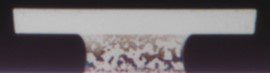 Fig. 1. 35 µm line with medium undercut, using sample processing conditions (see Table 1) with 2.5 minutes of development.
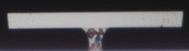 Fig. 2. 40 µm line with deep undercut, using sample processing conditions (see table 1) with 3 minutes of development.
The undercut profile of the bi-layer is primarily controlled by two steps: the soft bake step of the LOR layer, and the development step. Increasing the soft bake temperature of the LOR layer will decrease the undercut rate during the development step. This allows more precise control over the final undercut width, while increasing processing time for the development step.
For clean lift-off, Kayaku Advanced Materials recommends an undercut width-to-height ratio of 2:1. This ratio can be reduced by increasing the thickness of the top resist.
High Temperature, Thick Oxide Sputter Deposition
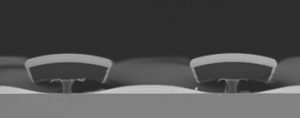 • 3.75 µm Ta2O5/SiO2 layer after high temperature (180˚C) deposition
• 8 µm UniLOR® N5.0 on top of 6 µm LOR 30C
• 35 µm L/S – 15 µm undercut
Minimal deformation highlighting the robustness of the bi-layer resist stack through the high stress deposition process
| Sample Processing Conditions | ||
| Dispense | 1 mL of resist for each inch (25 mm) of substrate diameter. | |
| Spin-coat LOR 30C | 500 rpm,
5-10 seconds, 500 rpm/s |
1400 rpm,
30 seconds, 1000 rpm/s |
| Soft Bake | 160°C/5 minutesa (hot plate) | |
| Film Thickness | 5.5 µm | |
| Spin-coat UniLOR® N5.0 | 500 rpm,
5-10 seconds, 500 rpm/s |
2500 rpm,
30 seconds, 1000 rpm/s |
| Soft Bake | 115°C/3 minutesa (hot plate) | |
| Film Thickness | 3.5 µm | |
| Exposure | 520 mJ/cm2 (with 360 nm long pass filter).
Intensity measured at 365 nm. |
|
| PEB | 120°C/4 minutes (hot plate) | |
| Development | MICROPOSIT® MF® CD-26 (0.26N TMAH).
Time depends on desired undercut. |
|
| Removal*
*Not used for Figures 1 and 2 |
30 minutes in Remover PG (NMP-based).
Time can be shortened with sonication. |
|
Table 1. Processing conditions for Fig. 1 and 2.
For a high temperature depositions (> 120˚C), the soft bake temperature of the LOR C and UniLOR® N should be increased to 200˚C and 125˚C, respectively.
FEATURED APPLICATIONS