Publications
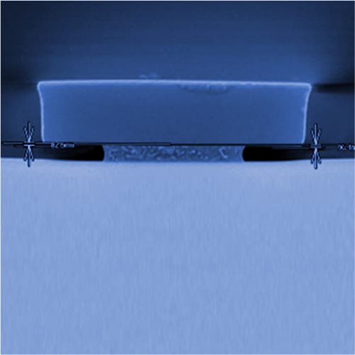
Bi-Layer Lift-off Resist Process Optimization of Insulator Film for Neural Probe Fabrication
Abstract The bi-layer lift-off method is used commercially to fabricate many MEMS and semiconductor device structures and is deployed for metallization processes to fabricate neural probe electrodes. The process utilizes LOR/PMGI plus an imaging resist to create a...
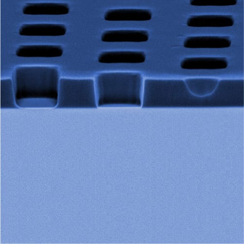
Optimization of Bi-layer Lift-off Resist Process
Abstract Bi-layer lift-off metallization techniques offer significant advantages in resolution, removal, process simplicity, undercut control and yield over conventional single-layer lift-off processes. Because of its ease of application, long shelf life and lower...
Novel Low Temperature Curable Photo-Patternable Low Dk/Df for Wafer Level Packaging
Sample publication excerpt


