


LOR & PMGI Lift-off Resists
Part of the StructSure® Line
PMGI and LOR resists enable high yield, metal lift-off processing in a variety of applications from data storage and wireless ICs, to MEMS. Used beneath photoresists in a bi-layer stack, PMGI and LOR extend the limits of lift-off processing beyond where single layer resist strategies can reach. This includes very high resolution metallization (<0.25μm), as well as very thick (> 3μm) metallization. These unique materials are available in a variety of formularies to meet virtually any customer need.

GaAs Modulator with Al Airbridge
Source: Nortel
PMGI used as a sacrificial layer on which the airbridge was built. The PMGI layer was subsequently removed with conventional resist removal processing.
Key Features
- Won’t intermix when over-coated with imaging resists
- Single step development of bi-layer stack in TMAH, or KOH developers
- High thermal stability: Tg ~190°C
- Removes quickly and cleanly in conventional resist strippers
- Enables sub 0.25μm micron bi-layer resist imaging
- Enables high yield, very thick (>3μm) metal lift-off processing
Material Uses
- Metal lift-off processing
- Airbridge fabrication
- Release layers
Lift-Off: An enabling, additive lithographic process
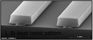
1. Bi-layer resist pattern
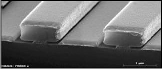
2. Metal Deposition
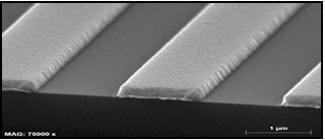
3. Clean solvent lift-off
Bi-Layer Lift-Off Process
Step 1. LOR or PMGI is coated
Step 2. The imaging resist is coated onto the LOR or PMGI layer.
Step 3. The imaging resist is exposed.
Step 4. The wafer is developed.
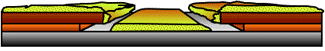
Step 5. Metal deposition
Step 6. Lift-off
LOR/PMGI Product Selection Guide

Broad Range of Products
