Photoresists & Specialty Chemicals
Lab-on-a-Chip
Part of the Applications Notes Line
As photoimageable bonding adhesives (PBAs), PermiNex® resists may be used for permanent and easy capping of silicon/glass structures, including microfluidic devices and MOEMS. Compared to direct bonding methods, PBAs allow lower temperature and pressure processing and simplified procedures (Fig. 1, Table 1). When compared with indirect bonding using standard photoresists, higher bonding strengths can be obtained in a single coat. These features make PBAs appealing materials for the quick fabrication of Lab-on-a-Chip devices (LOCs), analytical microsystems and other micro-devices.

Table 1. Characterization of various silicon/glass bonding methods
PermiNex™ Wafer Bonding Adhesives Attibutes:
- Permanent, photoimageable bonding resists
- Low temperature processing (< 200°C)
- High quality, void free bonding
- Superb adhesion to silicon and glass
PermiNex™ 2000 for the fabrication of a hybrid LOC for capillary gel electrophoresis (CGE)
CGE LOC design and fabrication
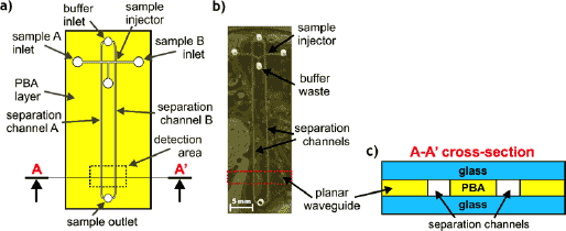
The developed PermiNex-glass CGE LOC enables simultaneous analysis of two genetic samples. It contains two symmetrical separation channels (32 mm long, 200 µm wide), two double-T sample injectors, and a common buffer inlet, waste and sample outlet (Fig. 2). All microfluidic components were fabricated in a single 14 µm thick layer of PermiNex™ 2000 on a glass substrate, utilizing standard photolithography. The PermiNex-glass structure was bonded to the top glass wafer containing vias. As fluorometric detection method was applied (DNA fragments were labelled with a fluorophore and detected at the end of the separation channel), and the PermiNex PBA layer also served as planar waveguide to couple the excitation light beam into the microchannels.
 Fig. 2. Hybrid CGE LOC for genetic analysis: a) top-view schematic of microfluidic components fabricated in PermiNex™ 2000 bonding adhesive layer, b) real-view of ready-to-use chip, c) cross-section scheme; PBA = PermiNex™ 2000 |
||||||||||||||||||||
|
||||||||||||||||||||
On-chip genetic analysis and results
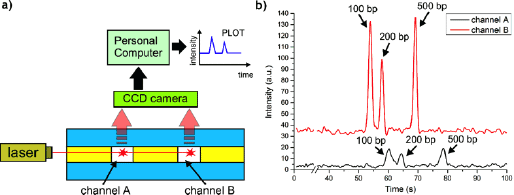
The analyzed genetic sample consisted of mixed double-stranded DNA fragments (100, 200 and 500 base pairs) labelled with Cy5 fluorophore. The microchannels were filled with POL-4 sieving matrix (A&A Biotechnology) and TBE was used as a running buffer. 1 µl of the sample was pipetted into each inlet, followed by electrohydrodynamic-driven transport, injection and separation (+800 V at sample outlet). Once separated, the DNA fragments passed through the detection area illuminated by laser beam, and the excited fluorophores produced peaks of fluorometric signal, which were acquired by a CCD camera and processed in PC into a plot of separation image (Fig. 3a).
For both samples, all DNA fragments were successfully separated and detected in less than 80 seconds (Fig. 3b). The relative migration time of the DNA fragments was similar in both separators, but an offset due to the formation of a small bubble in channel A was noted. The fluorescence signal was significantly higher in channel B due to the favorable dispersion of the beam on the side walls of channel A.
 |
| Fig. 3. a) schematic of fluorometric detection setup, b) results of simultaneous electrophoretic separation of DNA ladder samples (mix of 100, 200 and 500 base pairs (bp) fragments, each) in the developed hybrid CGE lab-on-a -chip |
| Application data and analyses are based upon the work of W. Kubicki, R. Walczak, and J. Dziuban (MEMSLab, Faculty of Microsystem Electronics and Photonics, Wroclaw University of Science and Technology, Poland) in collaboration with MicroChem Corp.
|

Fig. 1. Various schemes of silicon/glass bonding methods: a) direct bonding, b) indirect bonding using standard photoresist, c) indirect bonding using photoimageable bonding adhesive


