Photoresists & Specialty Chemicals
Wafer Thinning
Part of the Applications Notes Line
The wafer’s front surface containing the micro devices must be protected during the harsh wafer thinning/grinding and polishing of the back surface. PMMA coatings are useful as a protective bond and release layer for the front surface in wafer thinning. PMMA also affords protection during the subsequent dicing and handling steps. Its thermal and mechanical stability, as well as the ease of application, i.e. spin coating, and later removal in solvent, make PMMA a good candidate for this application.
The protective PMMA layer does not contaminate the active devices during mechanical processing nor leave residues or organic contamination prior to a final passivation.
PMMA: Benefits/Attributes
- Clean de-bonding
- Ease and efficiency of removal vs. wax
- Dual functionality: bonding and release layer
- Capable of withstanding various back-side processes:
– Lithography
– Etch
– CMP
– Metal Deposition:(Sputtering or Plating)
 Process Flow:
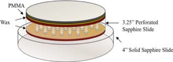
1. Coat 495 A15 onto the front-side of the wafer to a thickness of approximately 3µm and soft bake.
2. Coat wax onto the Solid Sapphire Carrier.
3. Affix the perforated Sapphire Carrier onto the softened wax layer.
4. Apply additional wax onto the perforated Sapphire Carrier and allow to melt.
5. Mount the PMMA-coated wafer onto the softened wax, PMMA-coated side down.
6. Back lap and polish the wafer.
7. Perform necessary back-side processing.
8. Dismount the wafer from the wax layer using heat and sliding it off the carriers.
9. Strip the PMMA in Remover PG at elevated temperatures. (25°–80° C)


 Process Flow: