KMSF® 2000 Low Dk/Df Photo-dielectric
Part of the StructSure® Line

KMSF® 2000 is a negative-tone, low-temperature cure, PPE-copolymer-based photo-dielectric for high reliability heterogeneous design in advanced packaging. It provides a unique advantage offering through its improved pattern resolution, low temperature cure, and robust balance of mechanical and electrical properties.
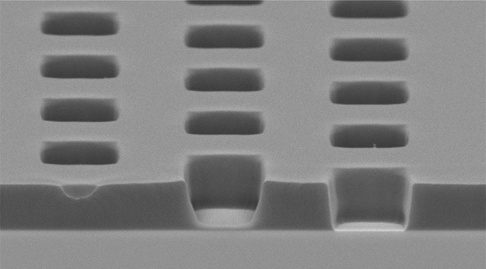
10 µm via
10 µm Film Thickness
KMSF® 2000 provides excellent performance with a low dielectric constant (Dk = 2.5) and a low dissipation factor (Df = 0.003), making it ideal for applications that require high-frequency reliability and signal integrity. It is engineered for an optimal cured film thickness of 5 to 10 μm, providing versatility and consistency in high-performance electronic packaging solutions.
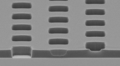
15 µm via
10 µm Film Thickness
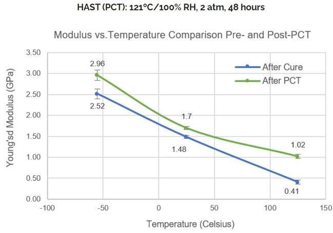
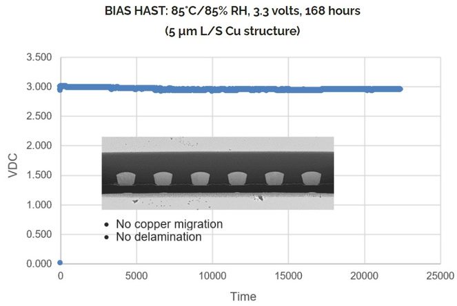
Cured Film Properties
| Process | |
|---|---|
| Available Viscosities | ~800 cSt ~1600 cSt |
| Mechanical Properties | |
| Young's Modulus | 1.6 GPa |
| Tensile Strength | 60 MPa |
| CTE α1 (<Tg) | 60 ppm/°C |
| Elongation | 65% |
| Residual Stress | 14 MPa |
| Electrical Properties | |
| Volume Resistivity | 6.7 x 10¹⁶ Ohm cm |
| Breakdown Voltage | 270 V/µm |
| Dielectric Constant (10-50 GHz) | 2.5 |
| Dielectric Factor (10-50 GHz) | 0.003 |
| Thermal Properties | |
| Tg (DMA) | 215°C |
| 5% Weight Loss Temperature in N₂ | 390°C |
| Water Absorption | |
| Moisture Absorption (23°C/85%RH, 24 hours) | 0.03% |
Key Features
- Negative tone, photoimageable dielectric
- 5 to 10 µm film thickness after cure
- Solvent-developable in PGMEA
- I-Line/broadband sensitivity, 1:1 aspect ratio imaging
- Low temperature cure ≤ 200°C
- Low Dk/Df electrical properties
- Low moisture uptake
- Good thermal and chemical stability
Material Uses
• RDL dielectric
• Passivation and protective layer
• Wafer level packaging

Process Parameters

Coat
KMSF® 2000 resist is available in two standard viscosities to cover a final cured film thickness of 5-10 µm. The post soft bake, as coated film thickness vs. spin speed, is displayed in Figure 2.
Please note the exact thickness obtained may be slightly offset from Figure 2. due to equipment type, setting differences and room conditions.
Recommended Program
1.Dispense 1 ml of resist for each inch (25 mm) of substrate diameter
2.Spin at 500 rpm for 5–10 seconds with acceleration of 500 rpm/second
3.Spin at 1000-3500 rpm for 30 seconds with acceleration of 500 rpm/second
Soft Bake
A 95°C soft bake for 2 to 4 minutes depending on the film thickness on a level hot plate with good thermal control and uniformity is recommended.
Exposure
KMSF® 2000 is compatible with i-Line and broadband exposure tools. Bulk film thickness loss associated with exposure and development is typically observed. A minimal broadband exposure dose of 250 mJ/cm2 (high pressure Hg vapor lamp) measured at 365 nm is recommended.

Development
KMSF® 2000 resist is optimized for development in PGMEA using immersion, spray, puddle, or spray/ puddle methods. For a 5 µm and 10 µm cured film thickness, 6 x 60 seconds puddle steps are recommended.
Bulk film thickness losses associated with the exposure and development are typically observed post development. Film loss and shrinkage data is depicted in Figure 4.


