

PMMA Positive Resists
Part of the StructSure® Line
PMMA (polymethyl methacrylate) is a versatile polymeric material that is well-suited for many imaging and non-imaging microelectronic applications. PMMA resists are simply PMMA polymer dissolved in a solvent like anisole (safe solvent). Exposure causes scission of the polymer chains. PMMA is most commonly used as a high resolution positive resist for direct write e-beam offering extremely high-resolution, ease of handling and excellent film characteristics. PMMA is also used as a protective coating for wafer thinning, as a bonding adhesive and as a sacrificial layer.
3 μm L/S in 3 μm thick UniLOR® N
Key Features
- Positive tone
- E-beam and X-ray imageable
- Wide range of film thicknesses
- Resist developers and strippers
- Excellent adhesion to most substrates
Material Uses
- High aspect ratio imaging of ultra-thick structures
- Vertical sidewalls
- i-line (365 nm) and broadband processing
- Improved adhesion
- Reduced coating stress
- 50 to 200 μm film thickness in a single coat
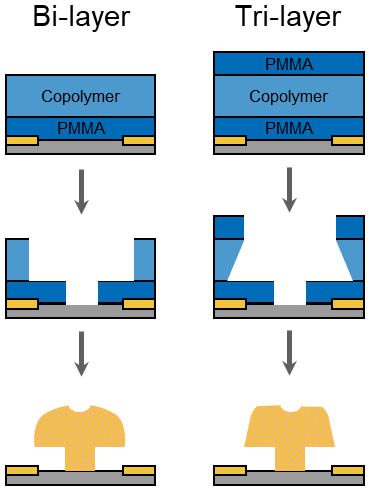
Copolymer resists are based on a mixture of PMMA and ~8.5% methacrylic acid. Copolymer MMA (8.5) MAA is commonly used in combination with PMMA in bi-layer lift-off resist process where independent control of CD size and shape of each resist layer is required. Standard copolymer resists are formulated in ethyl lactate and are available in a wide range of film thicknesses. All PMMA and copolymer resists are available in package sizes from 500ml to 20 liters.
Key Features
- Compatible with multi-layer processes
- Excellent adhesion to most substrates
Material Uses
- Multi-layer T-gate processes
- Other direct write e-beam processes
Application Notes
Schematic of T-Gate Illustrating Various Product Layers
Process Parameters
Coat
Kayaku Advanced Materials PMMA resists produce low defect coatings over a broad range of film thicknesses. The film thickness vs. spin-speed curves displayed in Fig. 2 through 11 provide the information required to select the appropriate PMMA dilution and spin speed needed to achieve the desired film thickness
Recommended Coating Conditions
1. Dispense: STATIC 5–8 ml for a 150 mm wafer
2. Spread: DYNAMIC 500 rpm for 5 seconds, or STATIC 0 rpm for 10 seconds
3. Spin: Ramp to final spin speed at a high acceleration rate and hold for a total of 45 seconds
Prebake
PMMA
Hot plate: 180ºC for 60-90 seconds, or
Convection Oven: 170ºC for 30 minutes
Copolymer
Hot plate: 150ºC for 60-90 seconds, or
Convection Oven: 140ºC for 30 minutes
*Vacuum oven bake can also be used
Exposure
PMMA can be exposed with various parts of the electromagnetic spectrum.
E-beam Dose: 50–500 μC/cm2 depending on radiation source/equipment & developer used.
Energy: 20–50 kV; higher kV for higher resolution, e.g. 50 kV for 0.1mm images.
X-ray: Sensitivity of PMMA is low, ~1-2 J/cm2 at 8.3 Å. The sensitivity increases at longer x-ray wavelengths. Features of <0.02 μm can be fabricated.
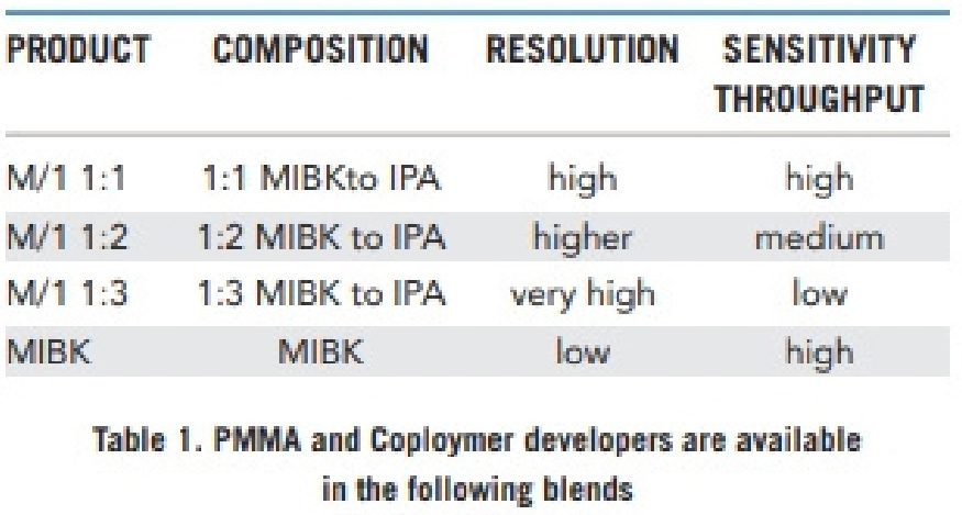
Development
PMMA and copolymer resists are compatible with immersion (21ºC), spray puddle, and spray process modes. Process variables such as soft bake, exposure conditions, choice of resist and developer should be optimized to achieve desired results. For more process details see the PMMA and Copolymer Developer data sheet. Table 1 lists commonly used developers and their recommended usage.